replacing the at 2S unreliable AMC7135s
DD + small FET and resistors instead
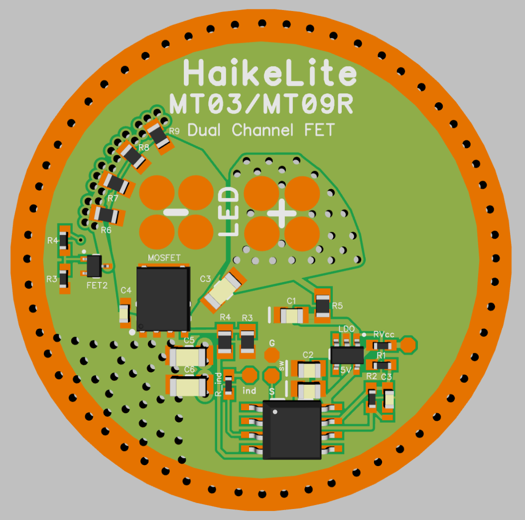
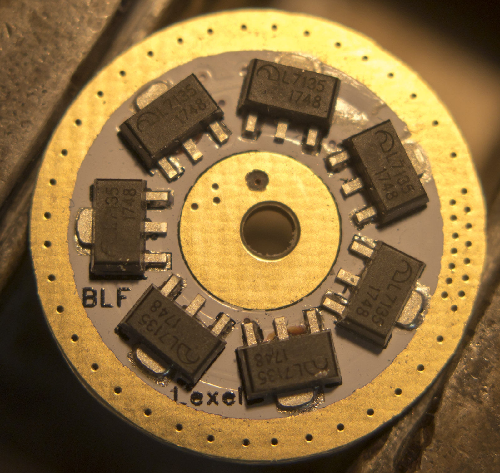
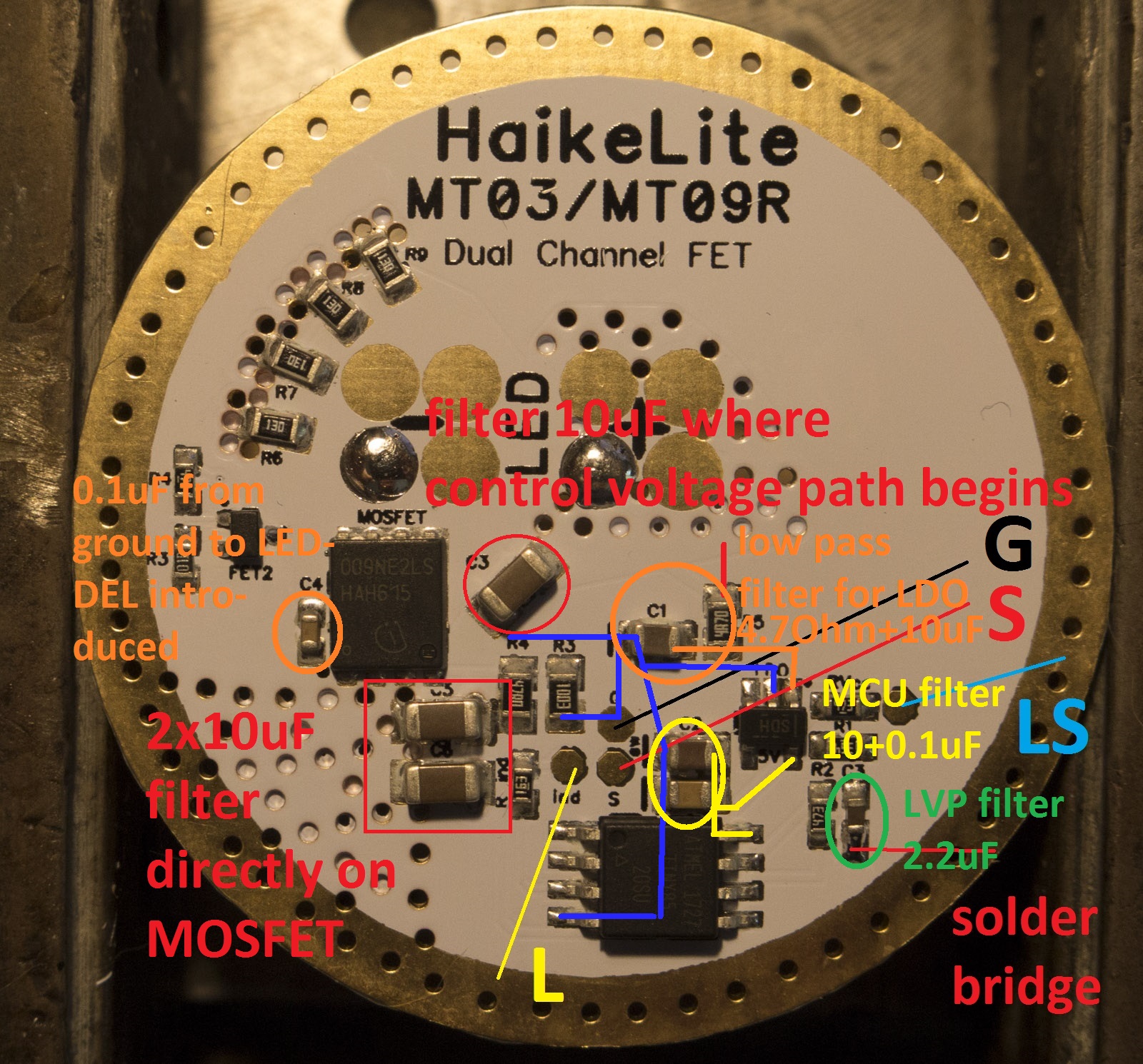
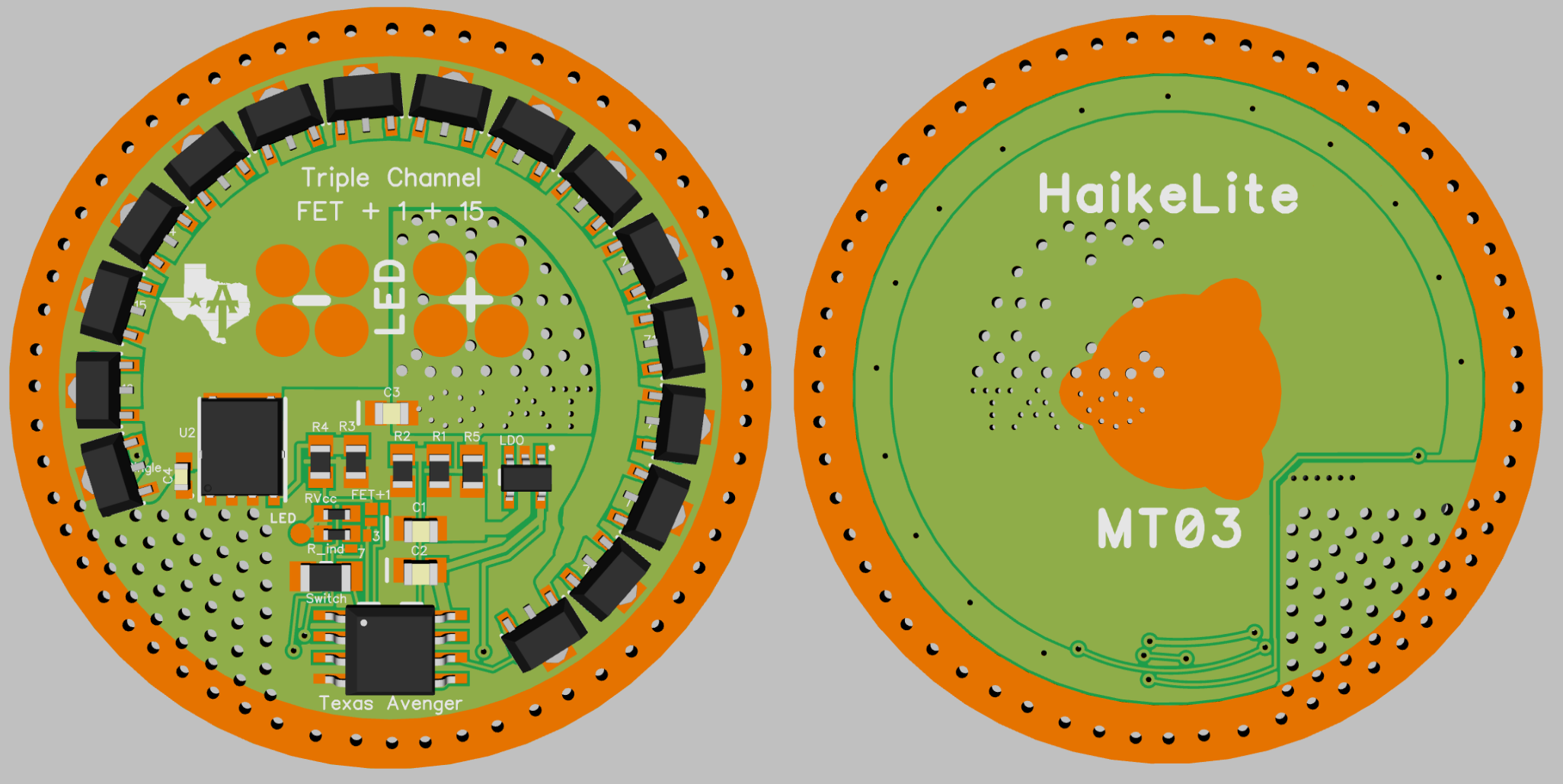
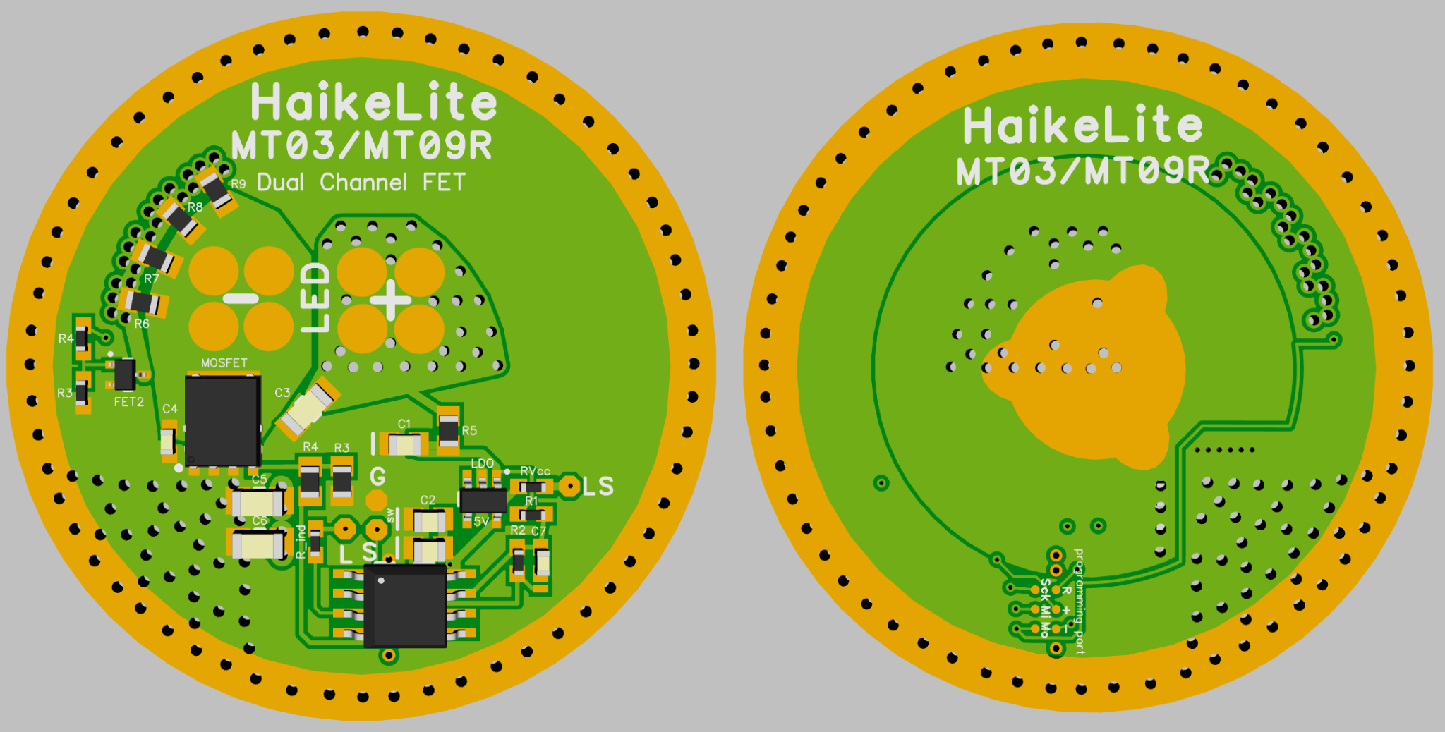
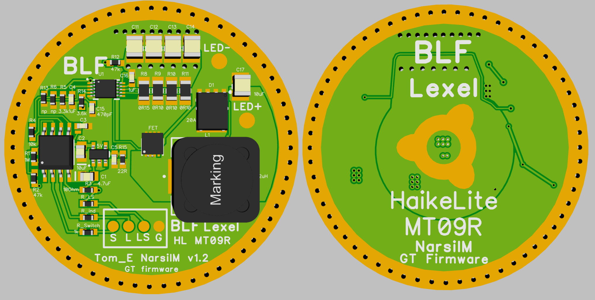
MT03/09R XHP70.2
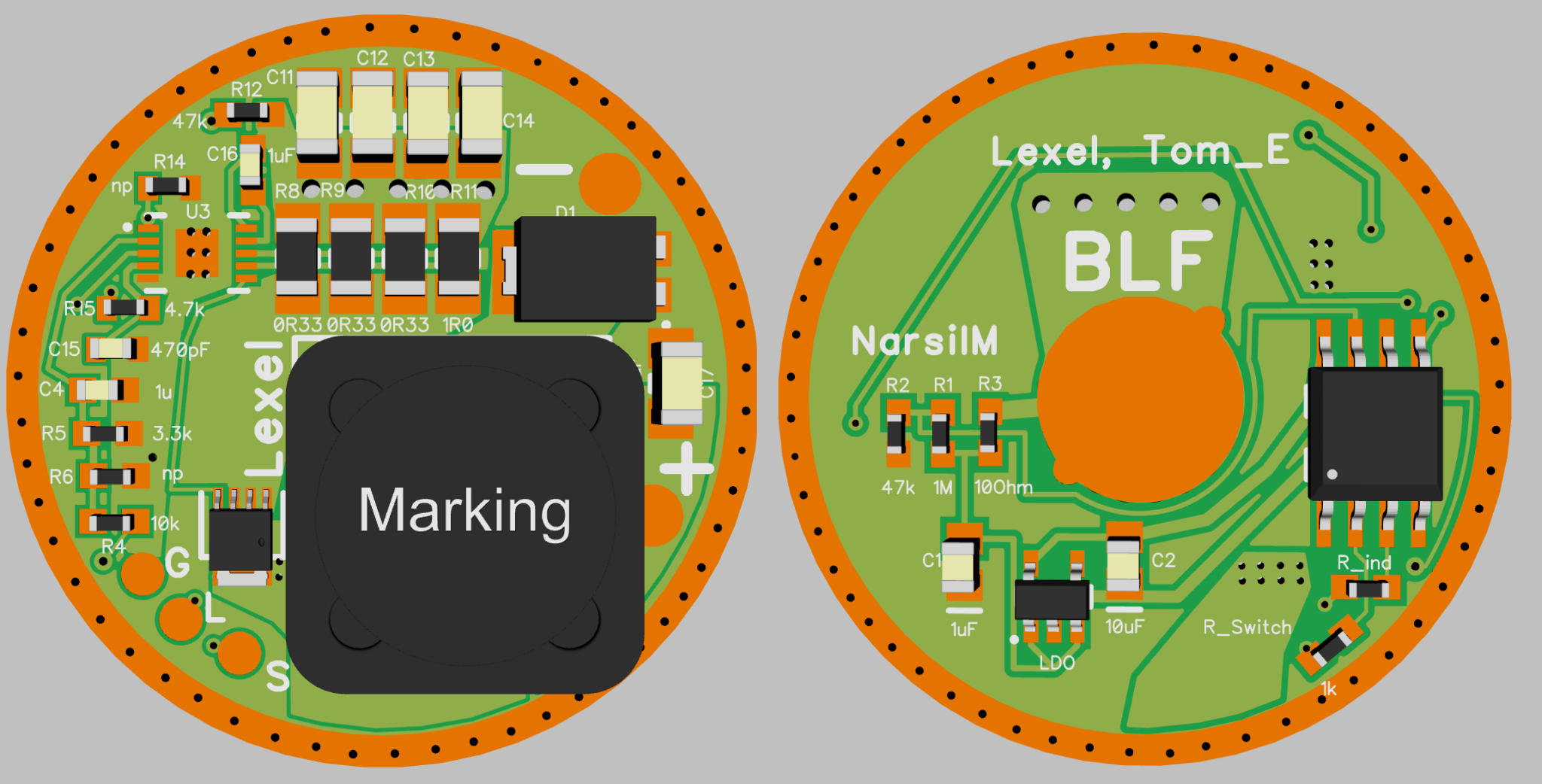
support of permanent switch LED plus MCU indicator with resistors
30mm for Convoy L6/ Thorfire S70S
support of permanent switch LED plus MCU indicator with resistors
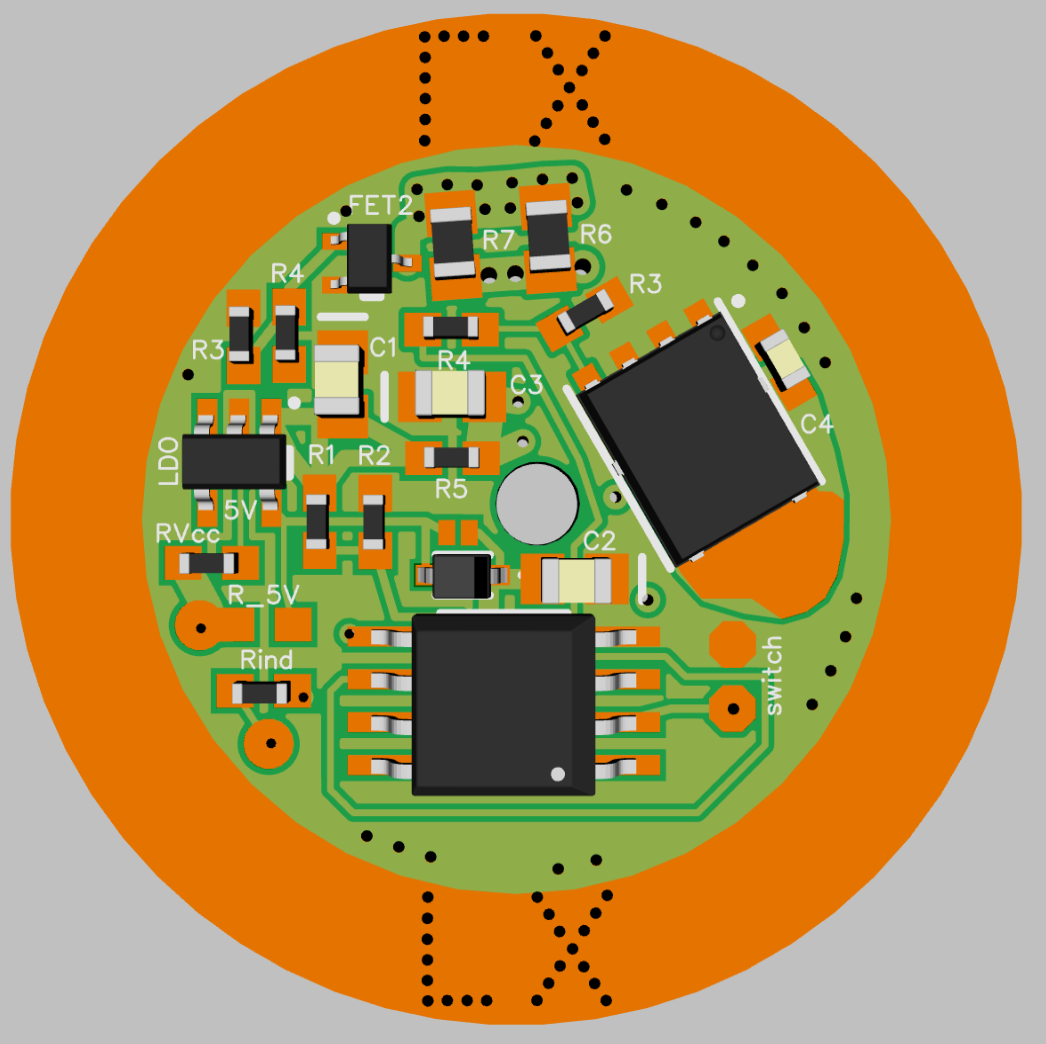
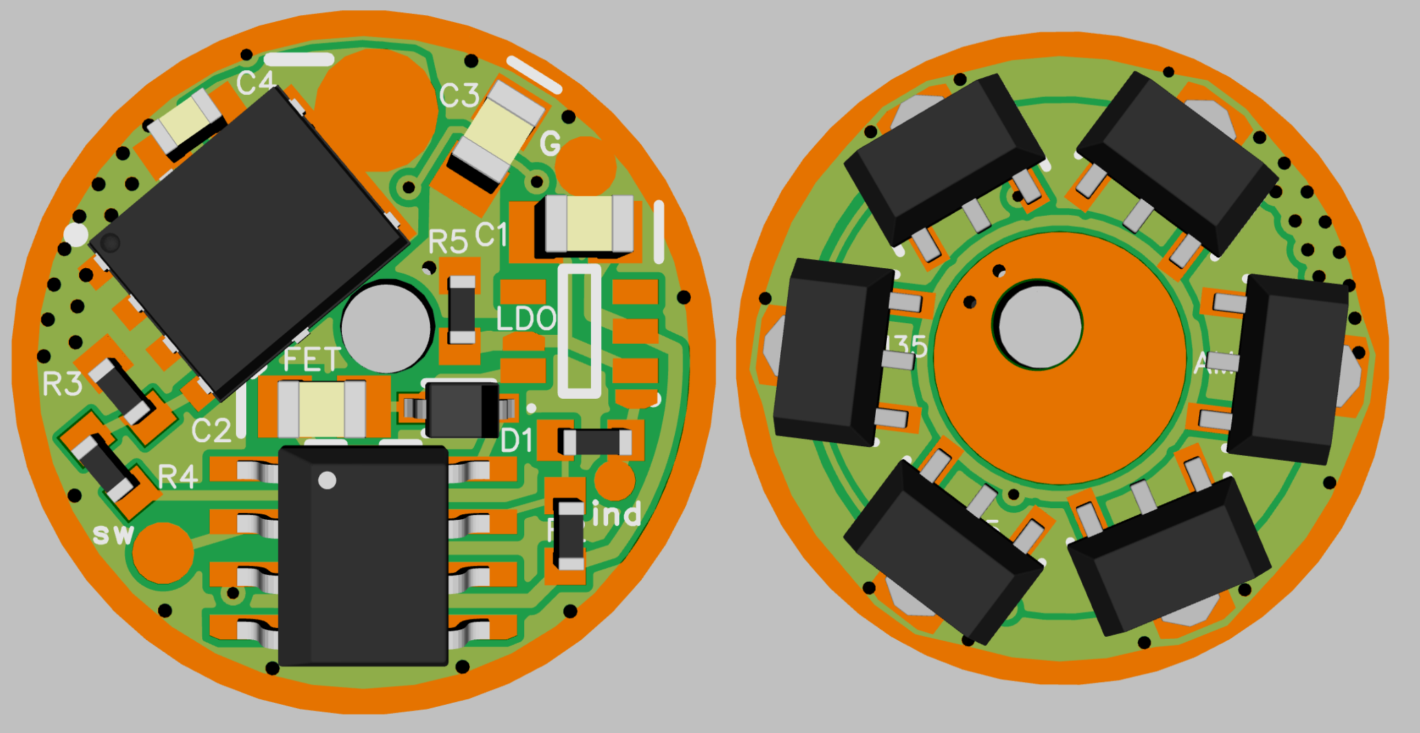
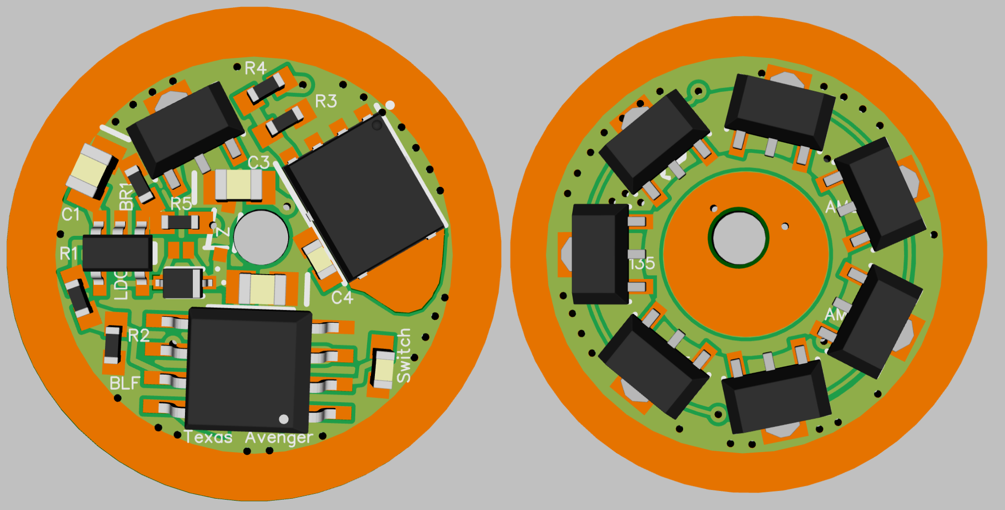
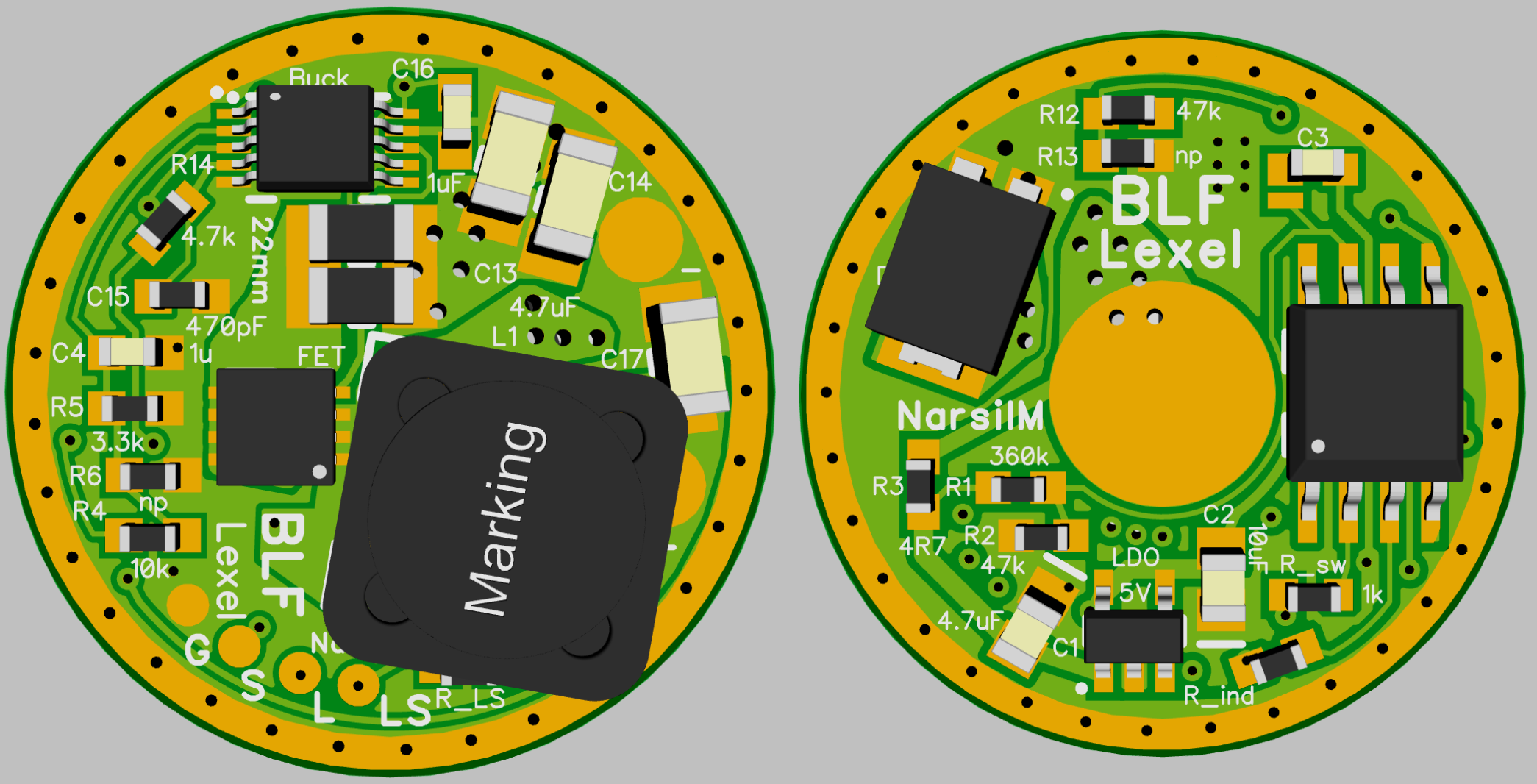
20-22mm with 2 FETs and also 6+1 AMC
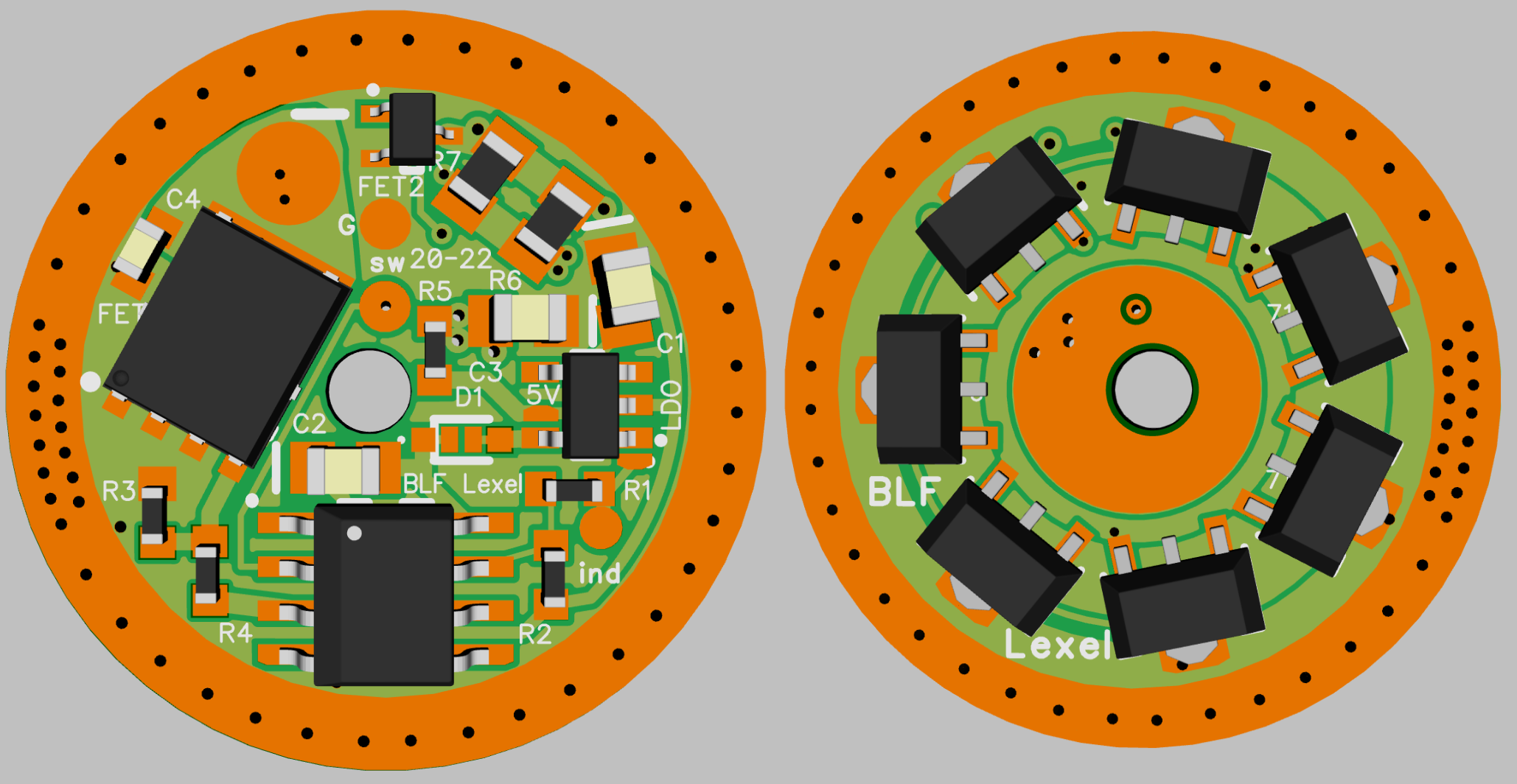
here with 1S configuration with 6+1 AMC
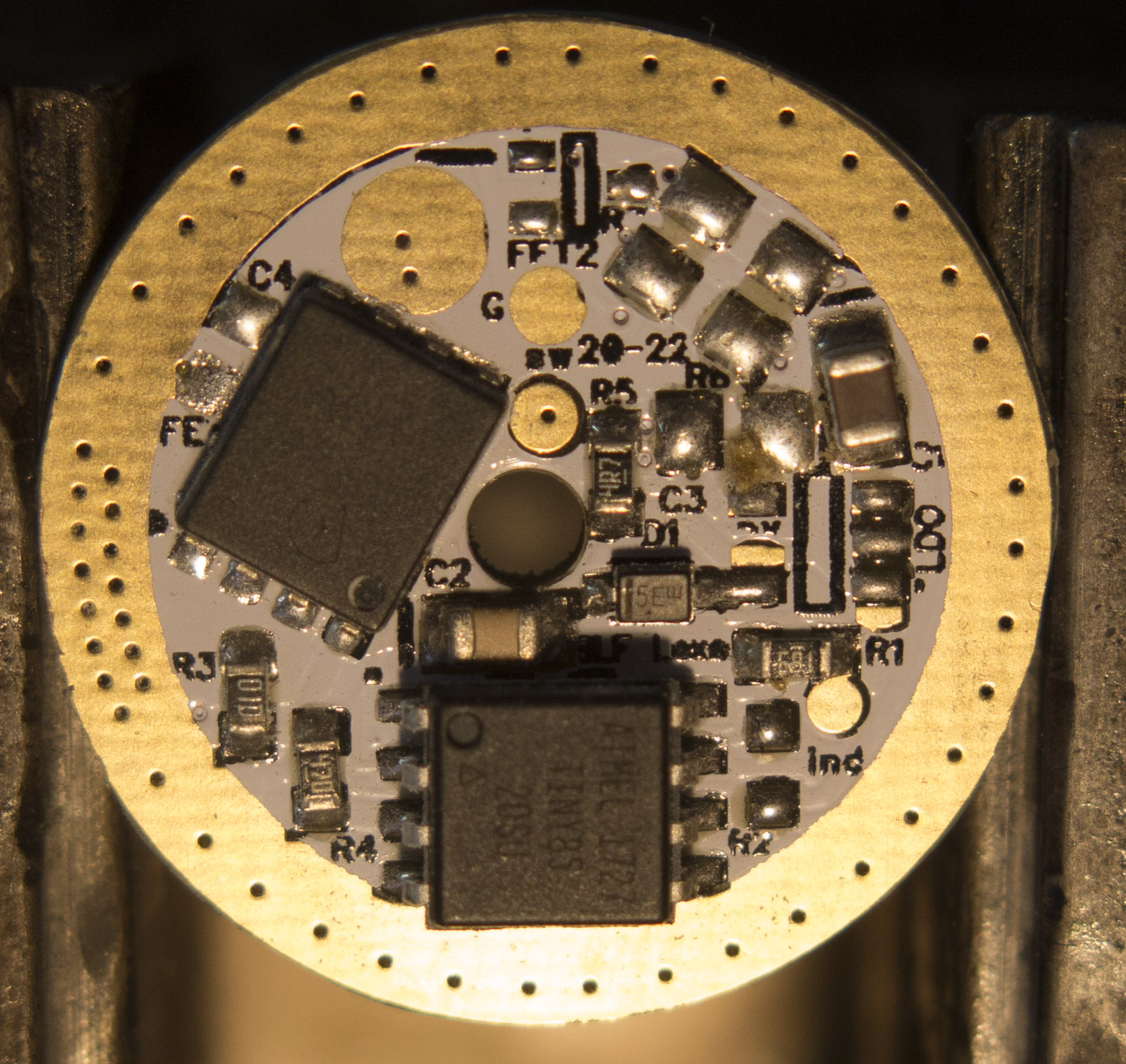
I had to drill out one via on the spring side partially that secures the switch pad from lifting if soldered too hot
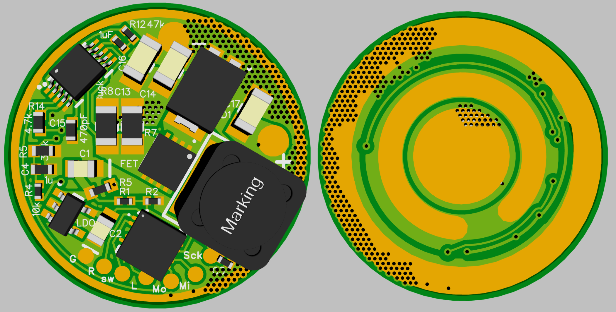
17mm 2S with 2 FETs
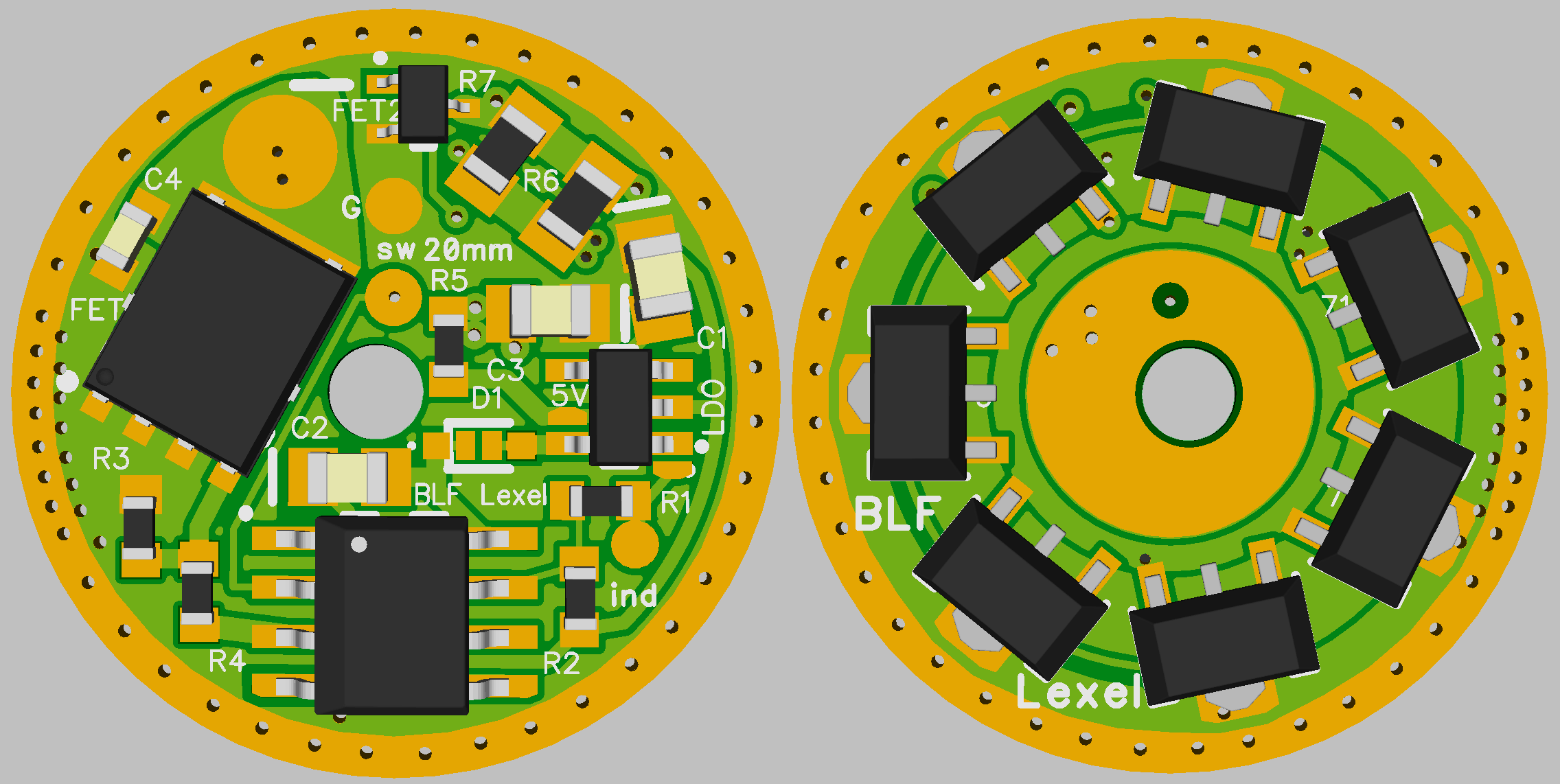
17mm LX v1.0 FET+5+1
more filtering caps for very high drain builds
Not sure where the best place to ask this is, so I’ll give it a try here. I had some boards made using: your ‘new’ 17mm TA layout. I built one in a 1s configuration with an ATTiny25v with no LDO, Zener or bleed resistor using recommended components and resistor values.
I flashed it with the bistro-TAv1-OTSM-HD-attiny25.hex file provided in the Bistro-HD v1.7.1 distribution.
It works great, except for one thing. The voltage readout is wrong. It usually reads out 4.2. I may have seen it go as low as 4.1.
My understanding is that the firmware I am using reads the voltage from Vcc. So I am really at a loss as to what could be wrong. My understanding is that 1.7.1 is pretty well tested for OSTM configs, but should I be using v1.4.1instead?
I got no idea what could cause this, I had never voltage readout making problems, sometimes the diode bridge was closed by solder paste and I got 4.4V readout
Thanks. I’ll have to refer to the schematics to better understand the extra caps.
I wonder if I bypassed the diode by mistake somehow. I cant remember how low I took the actual cell voltage. I know I haven’t tested it with low SoC cell, but I thought I’d check with a cell @ ~3.7.
I got atm not enough time to get ahead with the Boost, I made some progress just to run into a problem again
I ordered version 3 of prototyp boards 10 days ago, with enhanced thermal path to cool the MPS chip as I ran likely on 50W output into thermal problems I hope the new board will fix it
new 17mm for 2 S eliminating AMC7135 dedicated indicator resistor and pad
20mm new dual small FET and AMCs
20-22mm
new version with 1S 3 channel AMC and 2S dual MOSFET
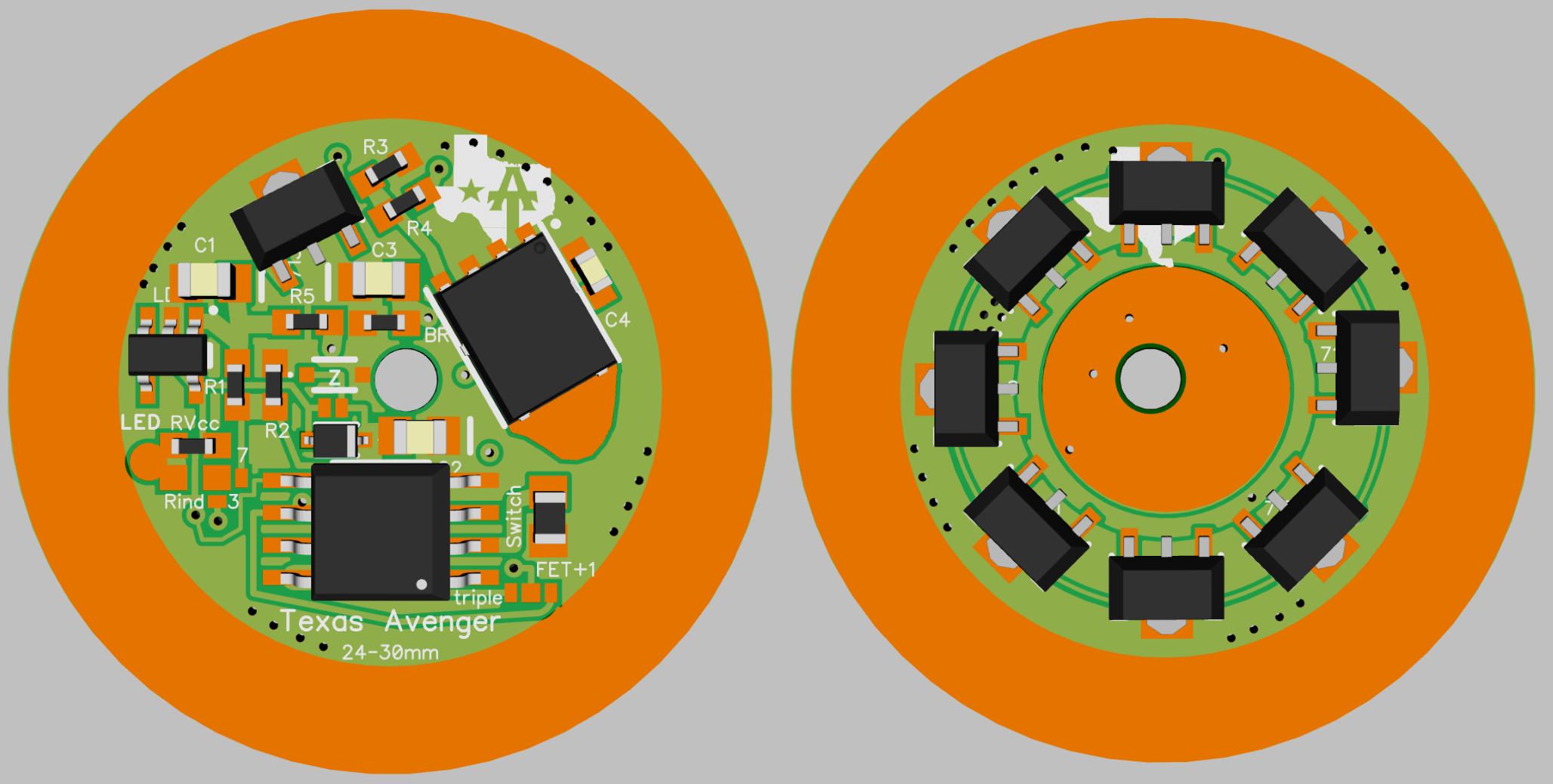
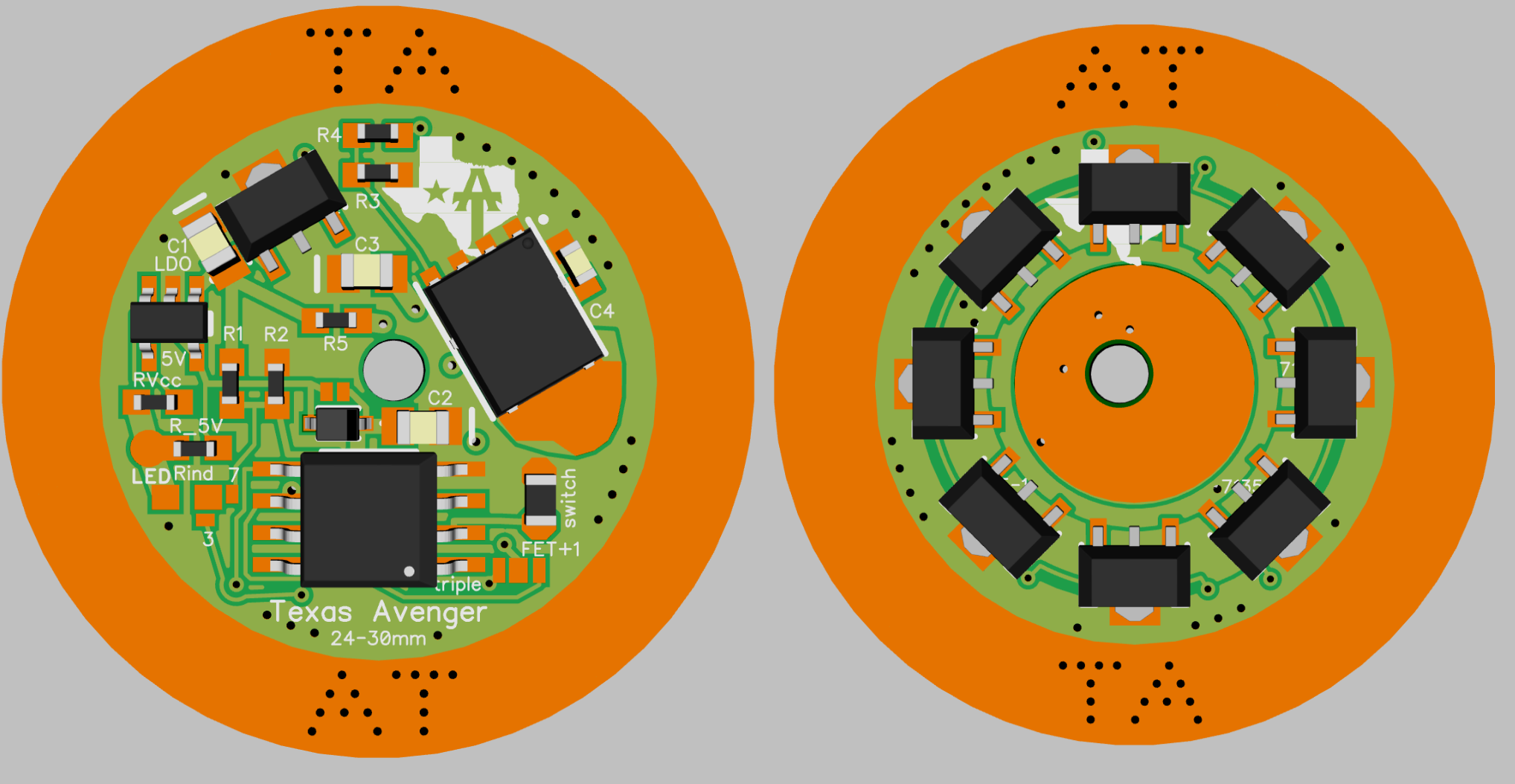
24-30mm
new design with added LED resistor to support new 2s 2x2 LED Boards and a little bugfix
new 2S version without AMC for more realibility, also added 2 switch LED support
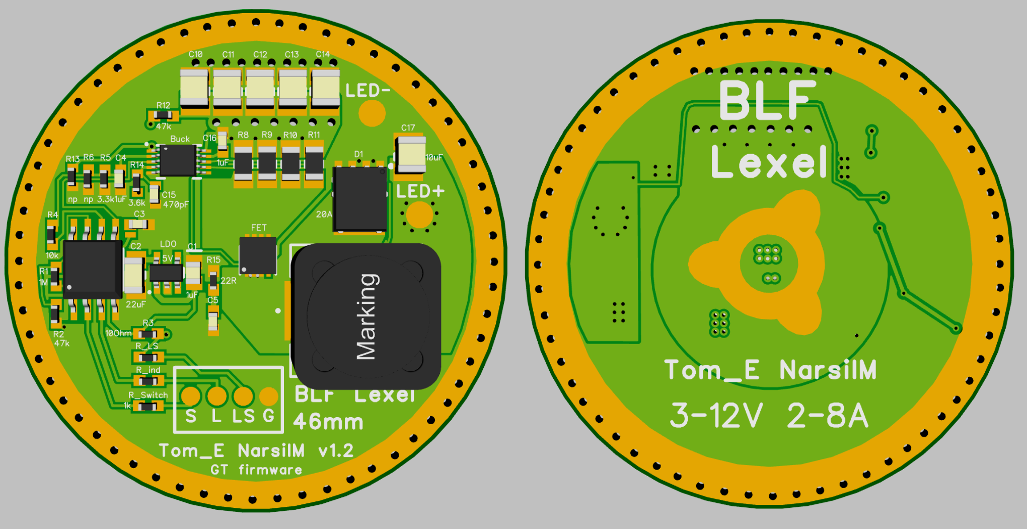
46mm 2S/2P MT03
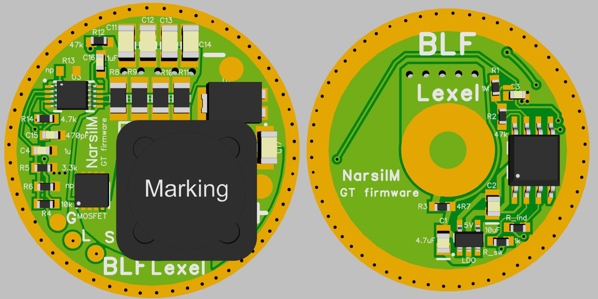
new enhanced version no more AMC7135
3 step filtering to get the rininging from PWM under control
.
Buck drivers:
20mm and 22mm
4 layer for better thermal properties
new more efficient MOSFET and minor changes
23mm for Klarus XT11/12GT running 2 18350s for Oslon BF or other 3V LED
30mm cheaper but bigger inductor
new with L6 compatible Ground ring and new MOSFET
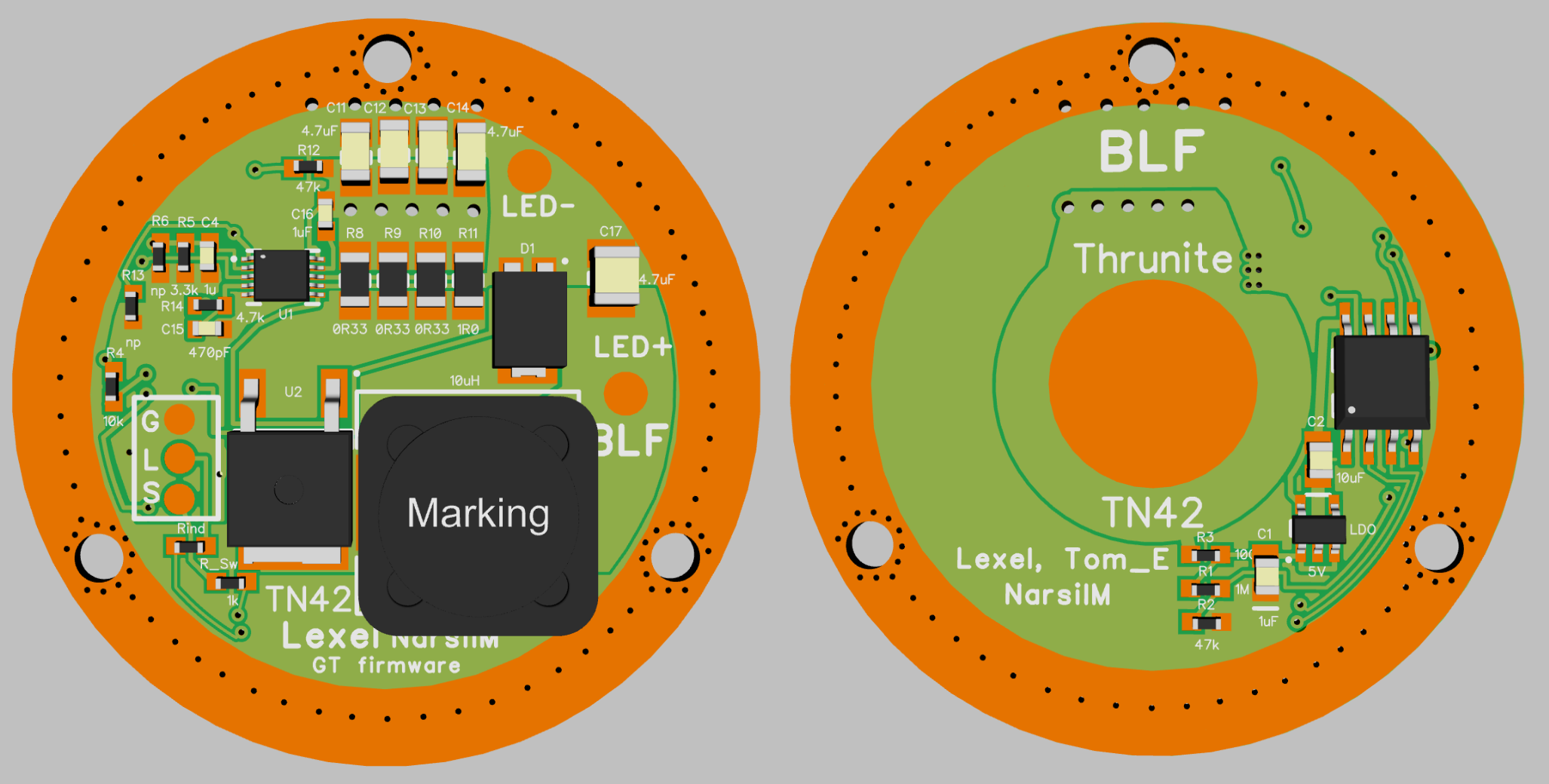
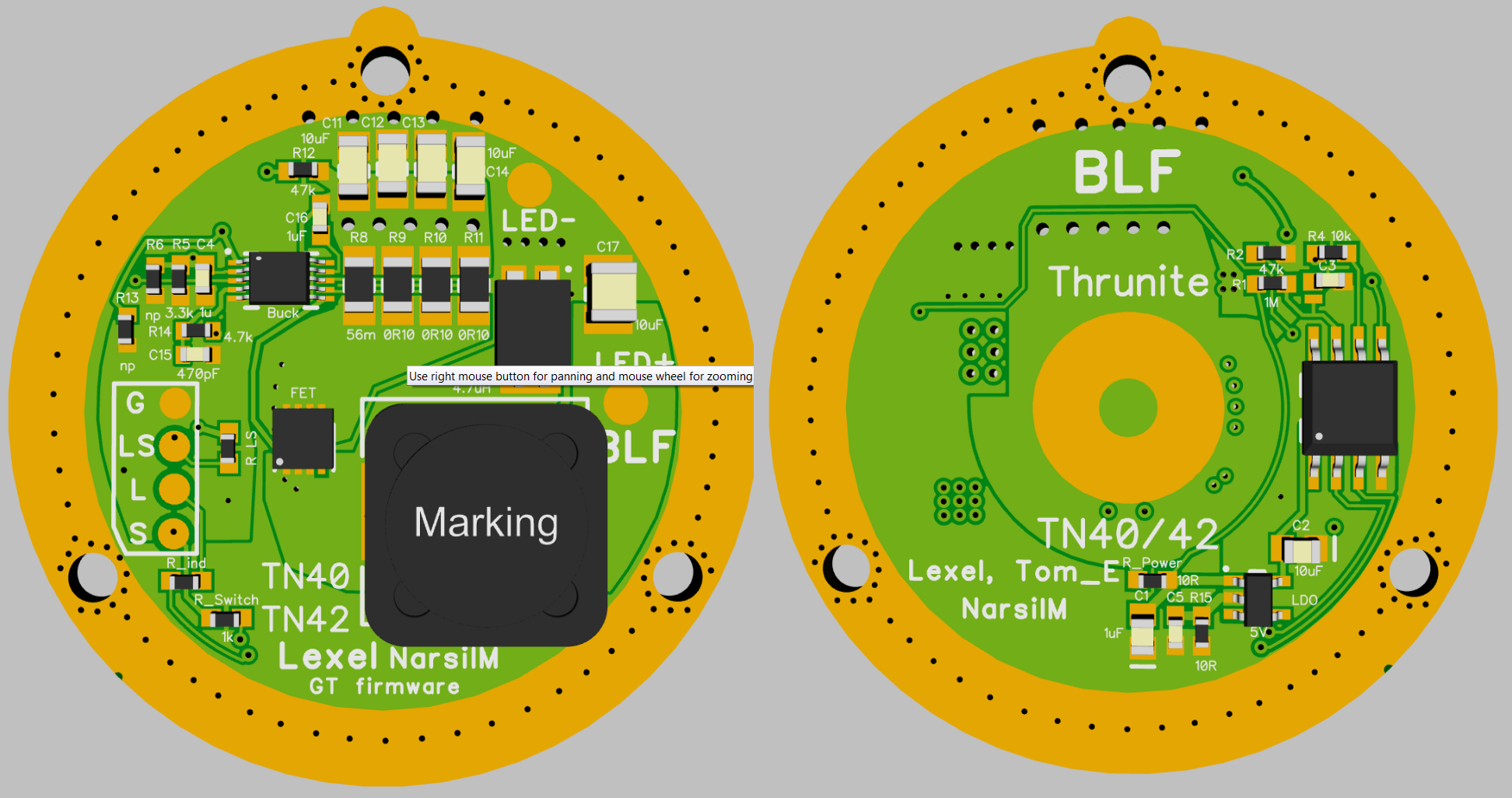
42mm TN42
new version up to 8A also for TN40S mods with XHP35s
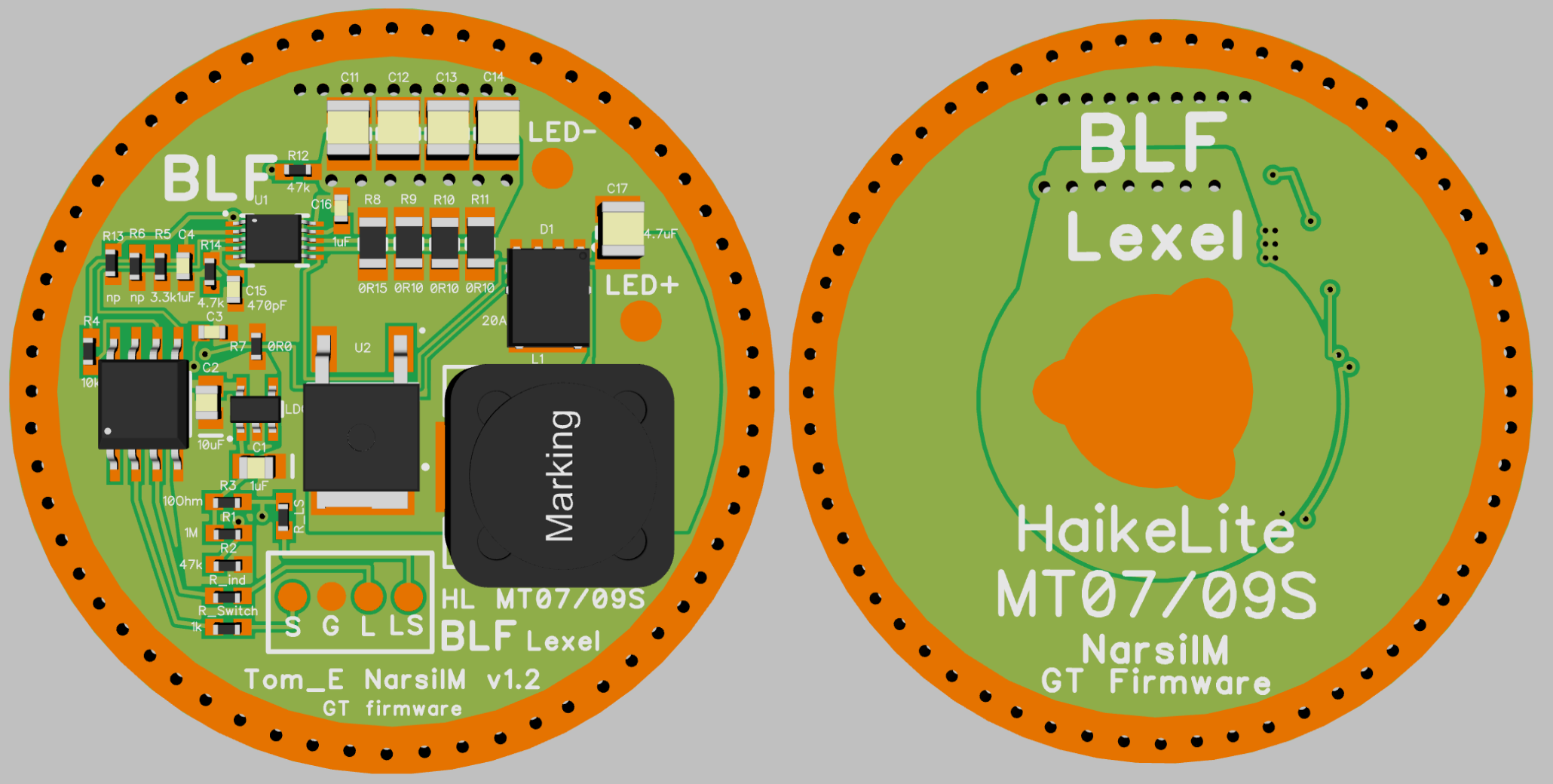
46 mm MT07/MT07S
new version a lot more efficient MOSFET
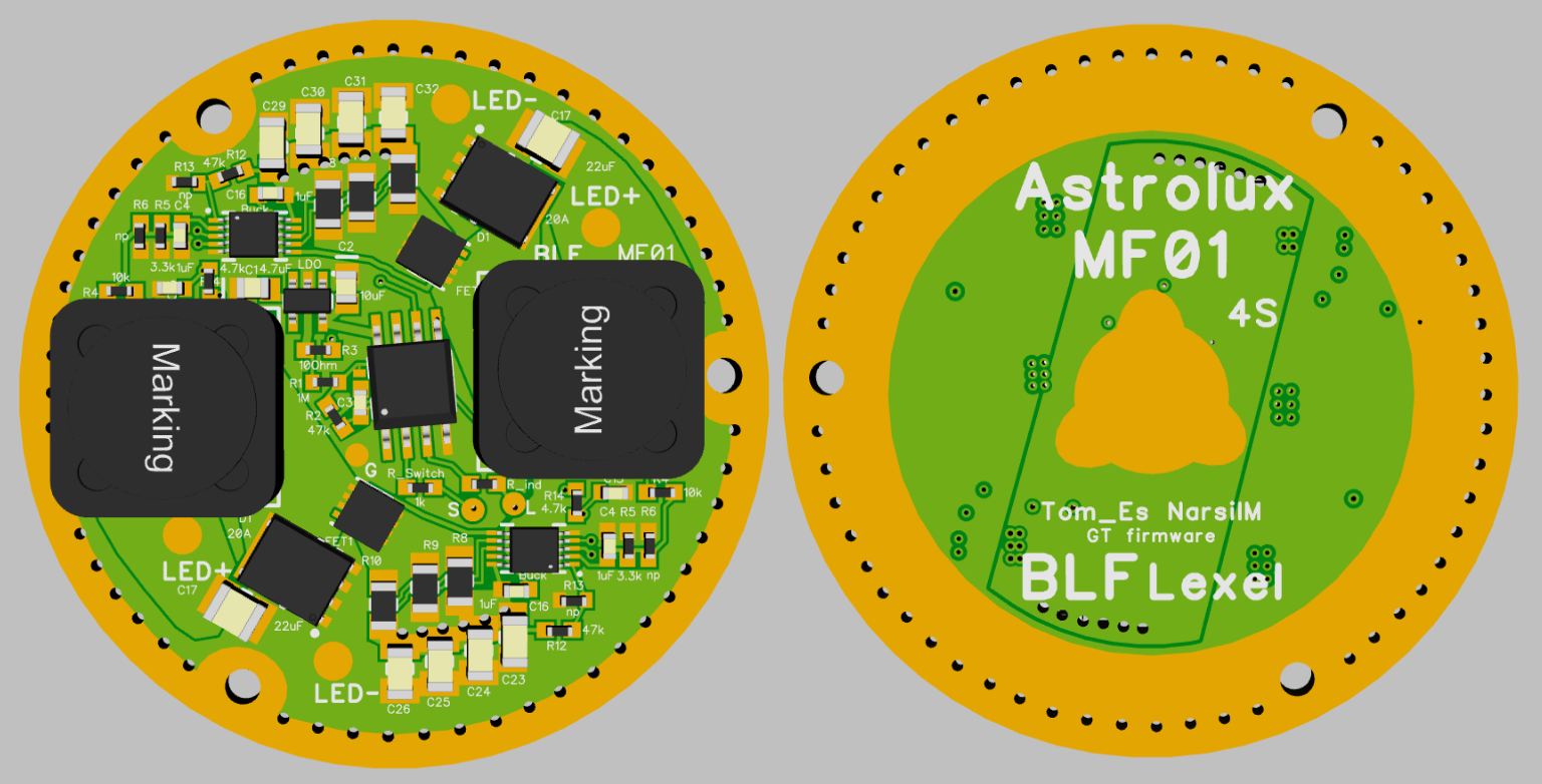
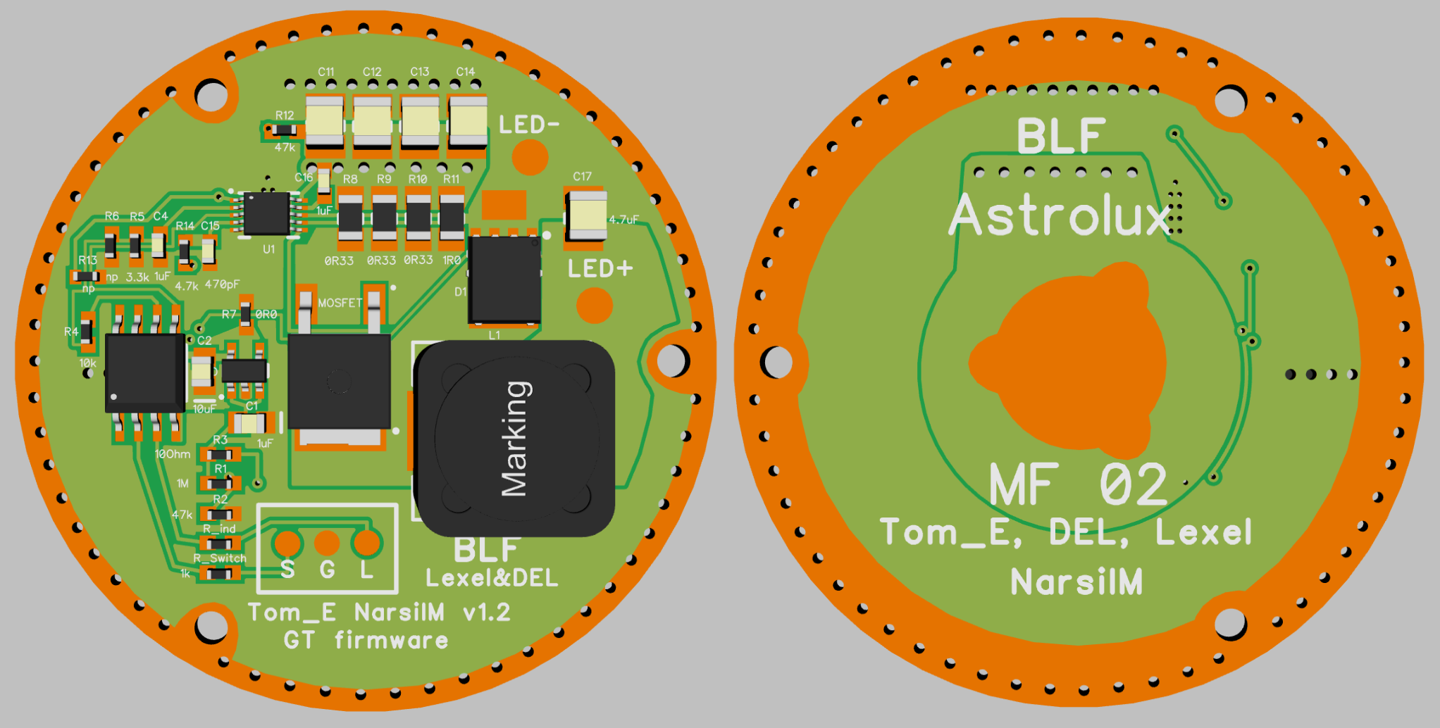
47,5mm MF02
new with better MOSFET and a lot imptrovements
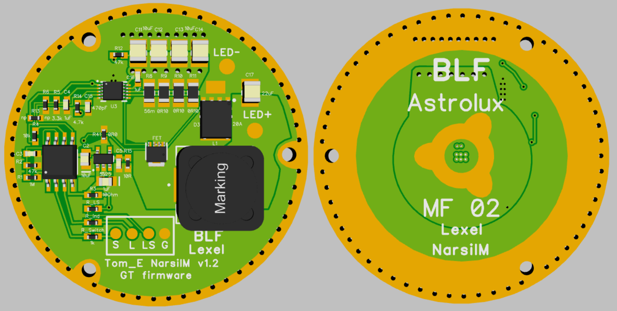
46/47,5mm 2S/2P or 4S/1P AstroluxMF01/ Haike LiteMT03
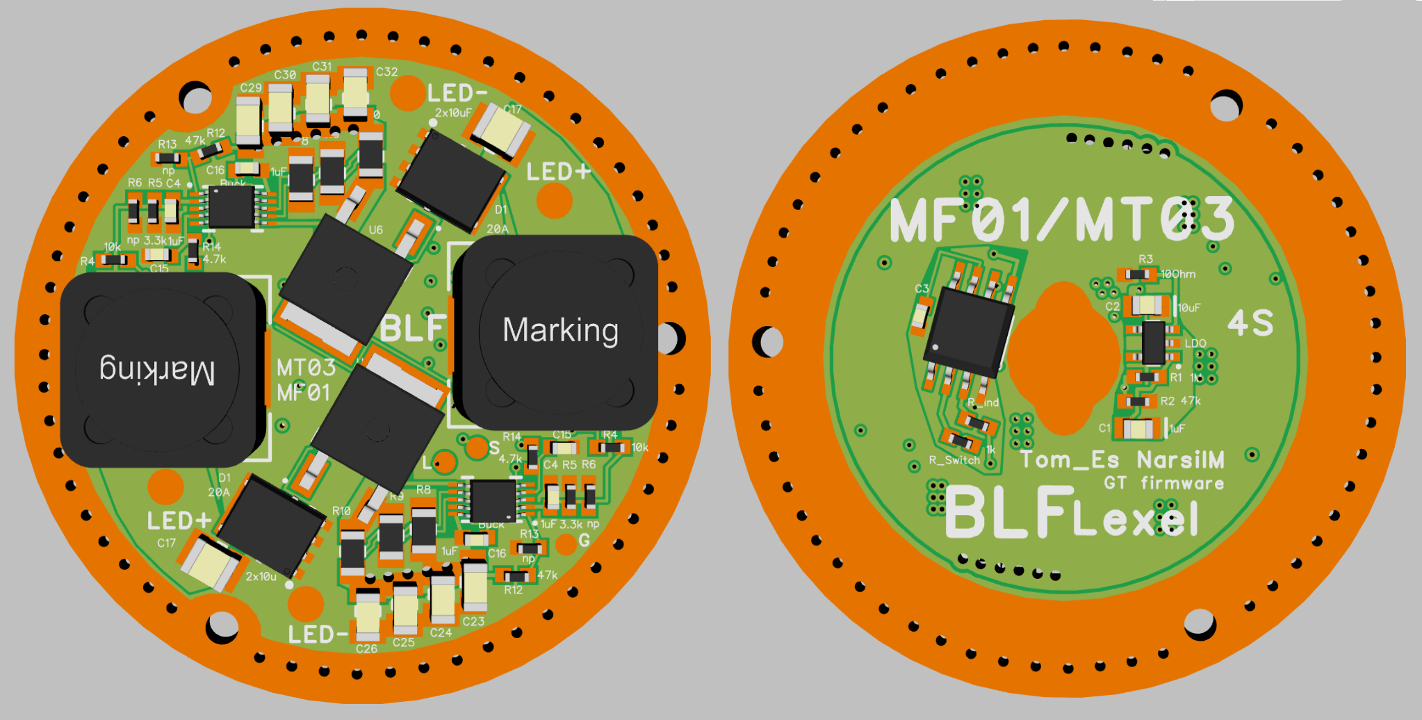
MF01 v2 in 3S/6P LED Board mod, driver has 4S input 3S Output
MF01 v2 3S 14A dual Buck driver with new MOSFET and now single sided
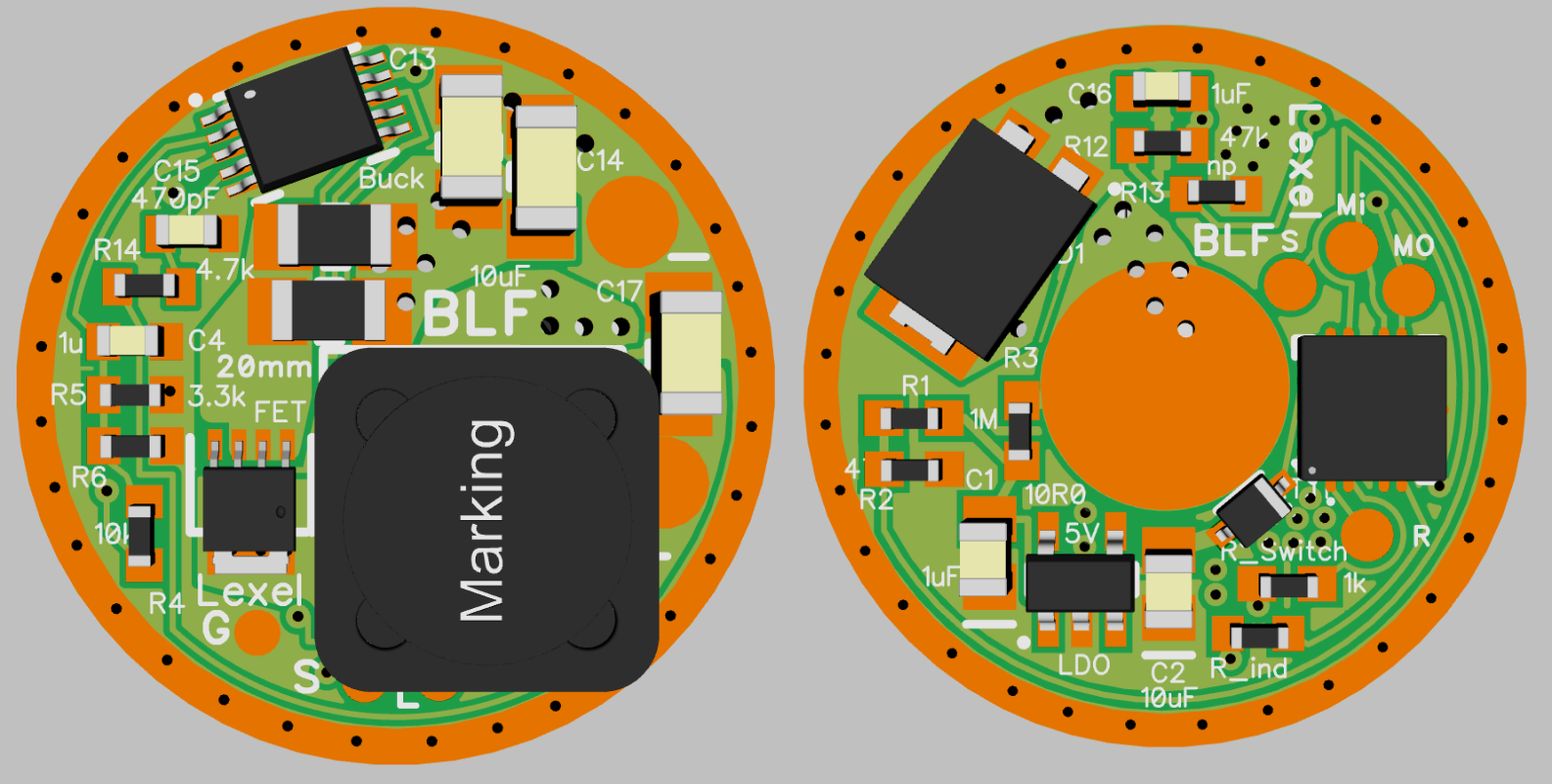
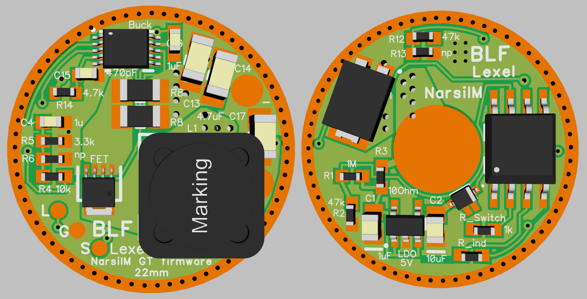
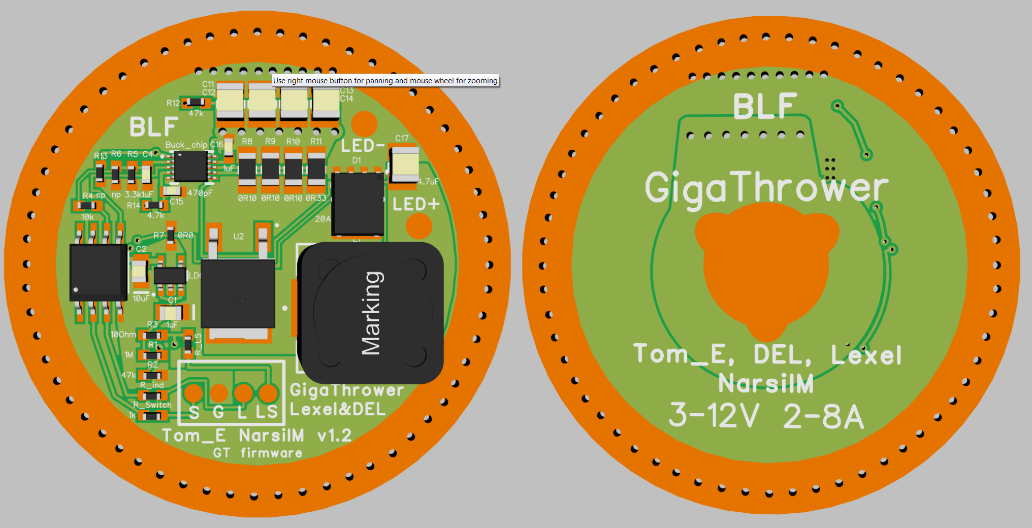
BLF GigaThrower driver
XHP70.2 or Oslon Black Flat up to 8A
new version
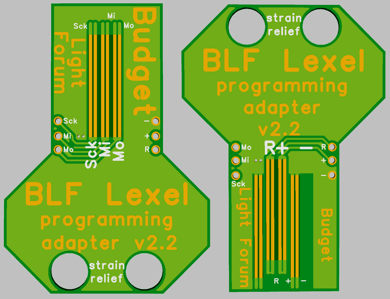
also made a programming adapter for my future drivers
same order in 2 Oz from Oshpark that gives 0.8mm thickness
So I think final version of programming port found
rearranged pins to fit MCU pins arrangement better than original v1.0 had
improvement machanically
2 traces on the pogo pin board to self align it by the solder
increased pad size on drivers to 0.8mm, to compensate wrong pogo pins
length of the solder traces on board reduced as some flux went in the pogo top, can be solved with alcohol but more distance is better
Added a key head for easier handling
added 2 holes to use a wire strap to secure the programming wire
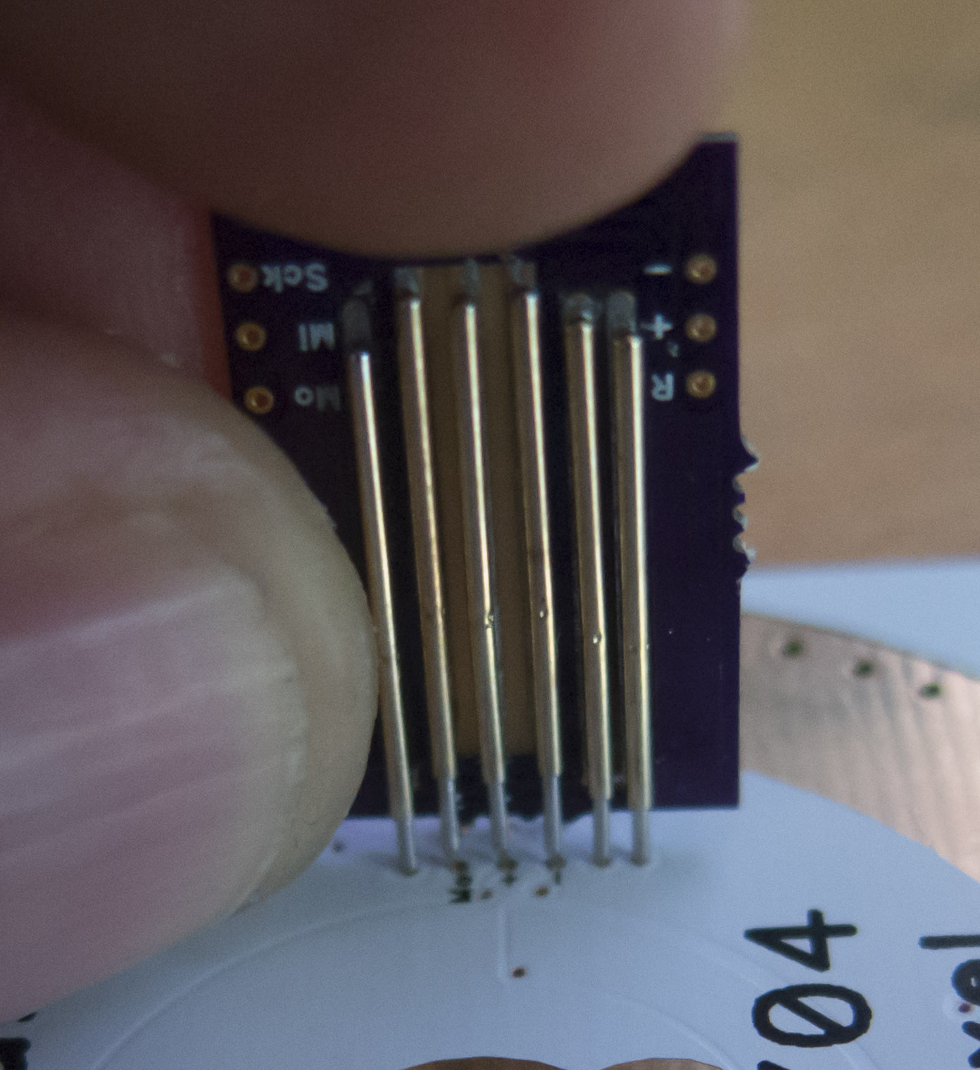
Picture of v1.1 on V1.0 board, pin alignment does not work on the small 0.6mm pad on first reflow