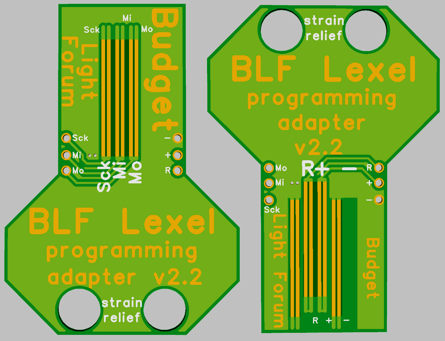
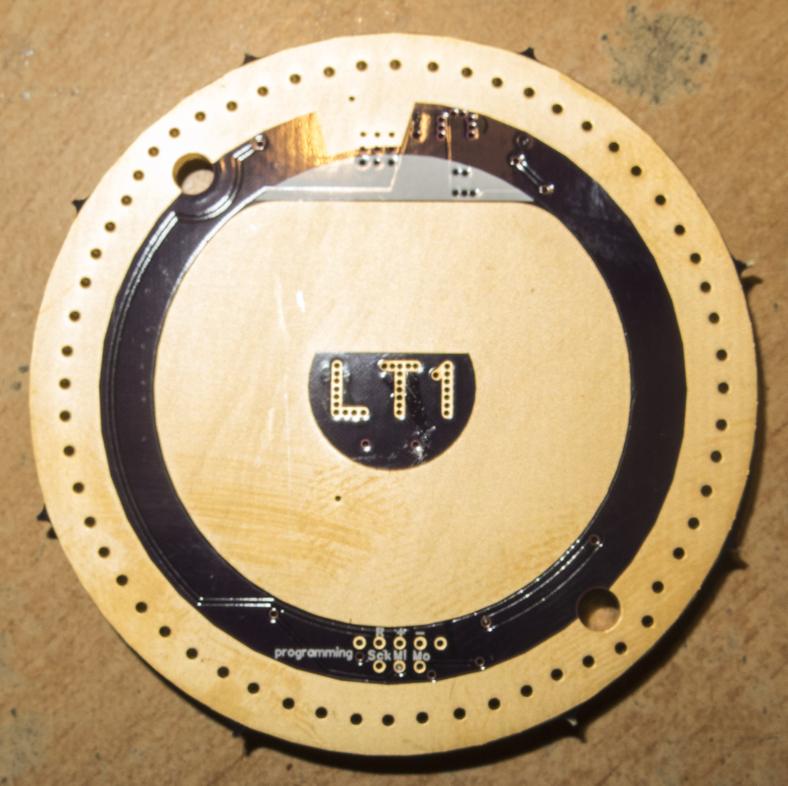
So I think final version of programming port found
rearranged pins to fit MCU pins arrangement better than original v1.0 had
improvement machanically
2 traces on the pogo pin board to self align it by the solder
increased pad size on drivers to 0.8mm, to compensate wrong pogo pins
length of the solder traces on board reduced as some flux went in the pogo top, can be solved with alcohol but more distance is better
Added a key head for easier handling
added 2 holes to use a wire strap to secure the programming wire
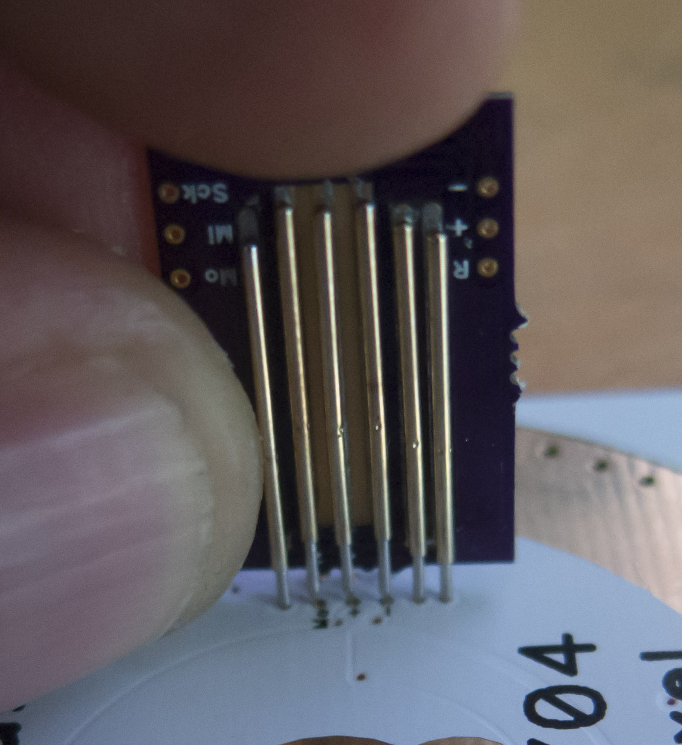
Picture of v1.1 on V1.0 board, pin alignment does not work on the small 0.6mm pad on first reflow
over time new ones, but I have here hundreds of old boards stocked up, likely 600-800
so if I take a new board over an old I would charge something, as I am usually try to use older designs if the performance is the same
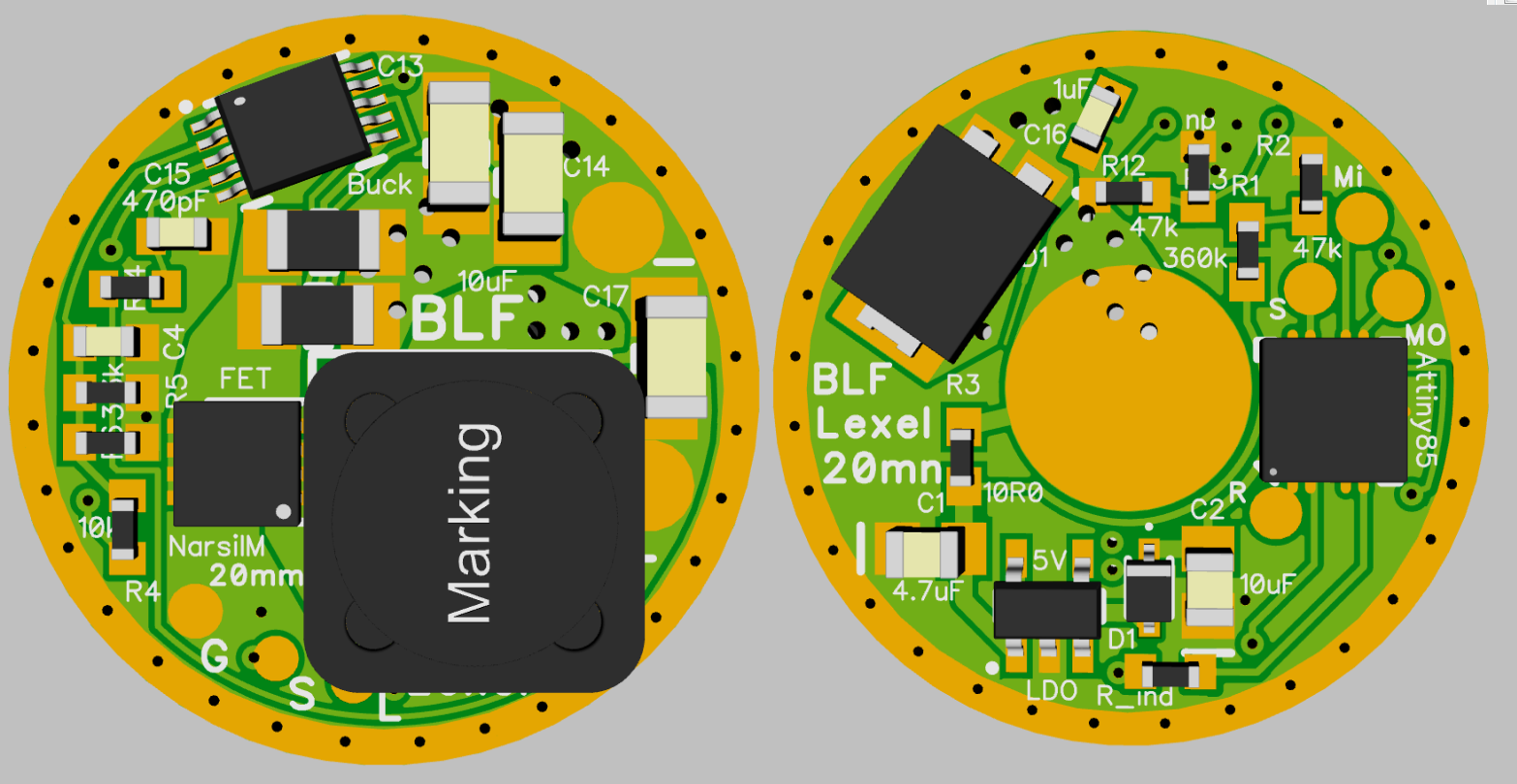
If a board got new MOSFET like on the Buck I am sitting on dead boards and parts if noone want a XHP35 Buck driver, where old parts have no disadvantage
I even cancelled the current enhancement fee for high power parts, but those 6-8A all get all new parts
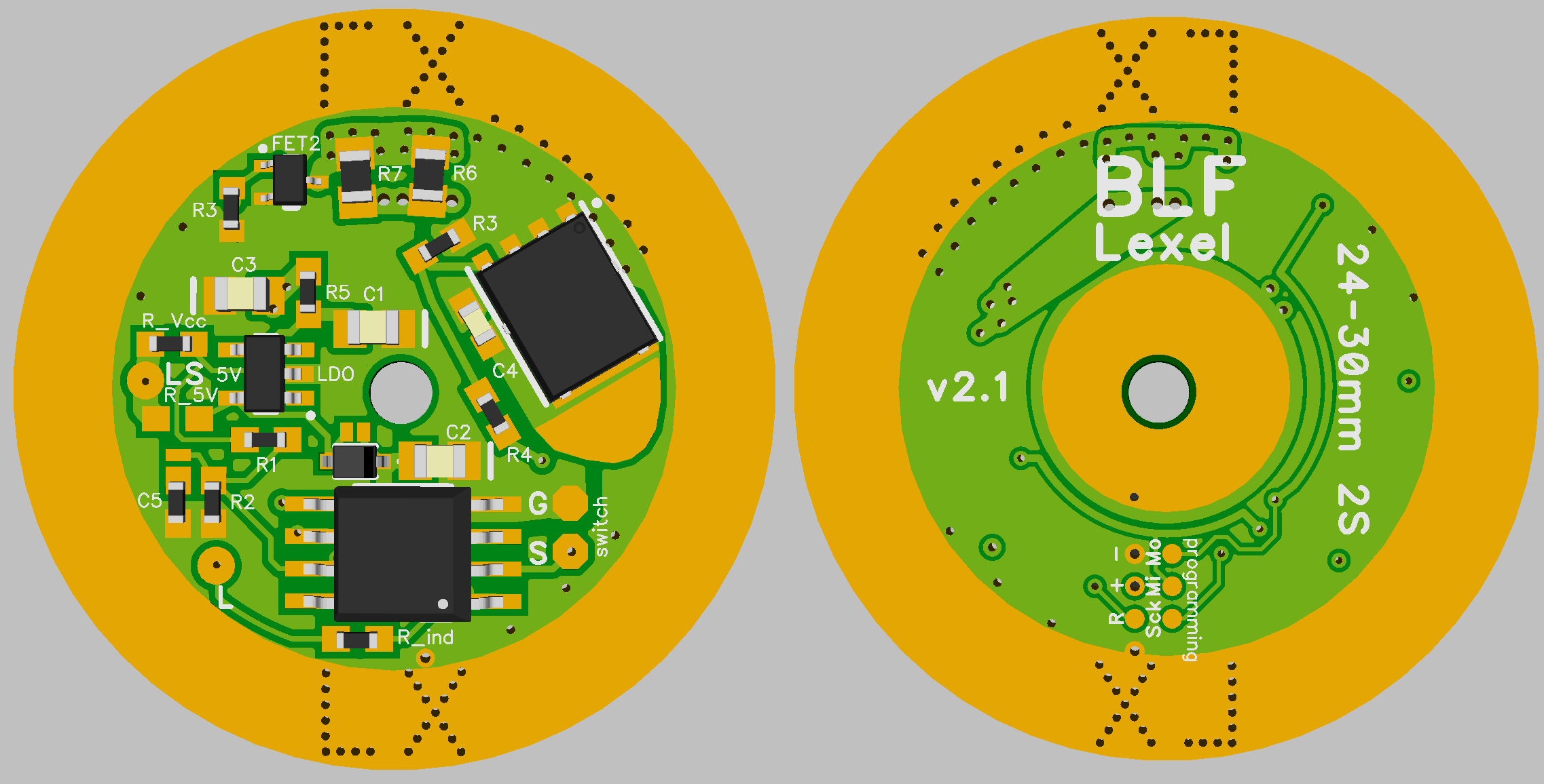
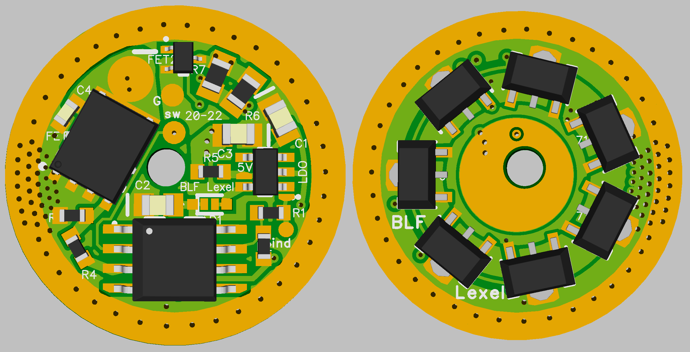
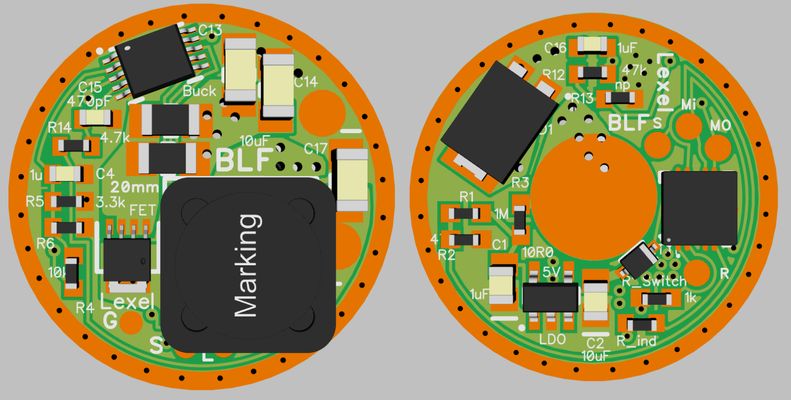
LX has nothing to do with TA, its complete new drawn design with all my previous tweaks
its based on Narsil Triple channel/Bistro HD OTSM of course the end product is similar in some ways
.
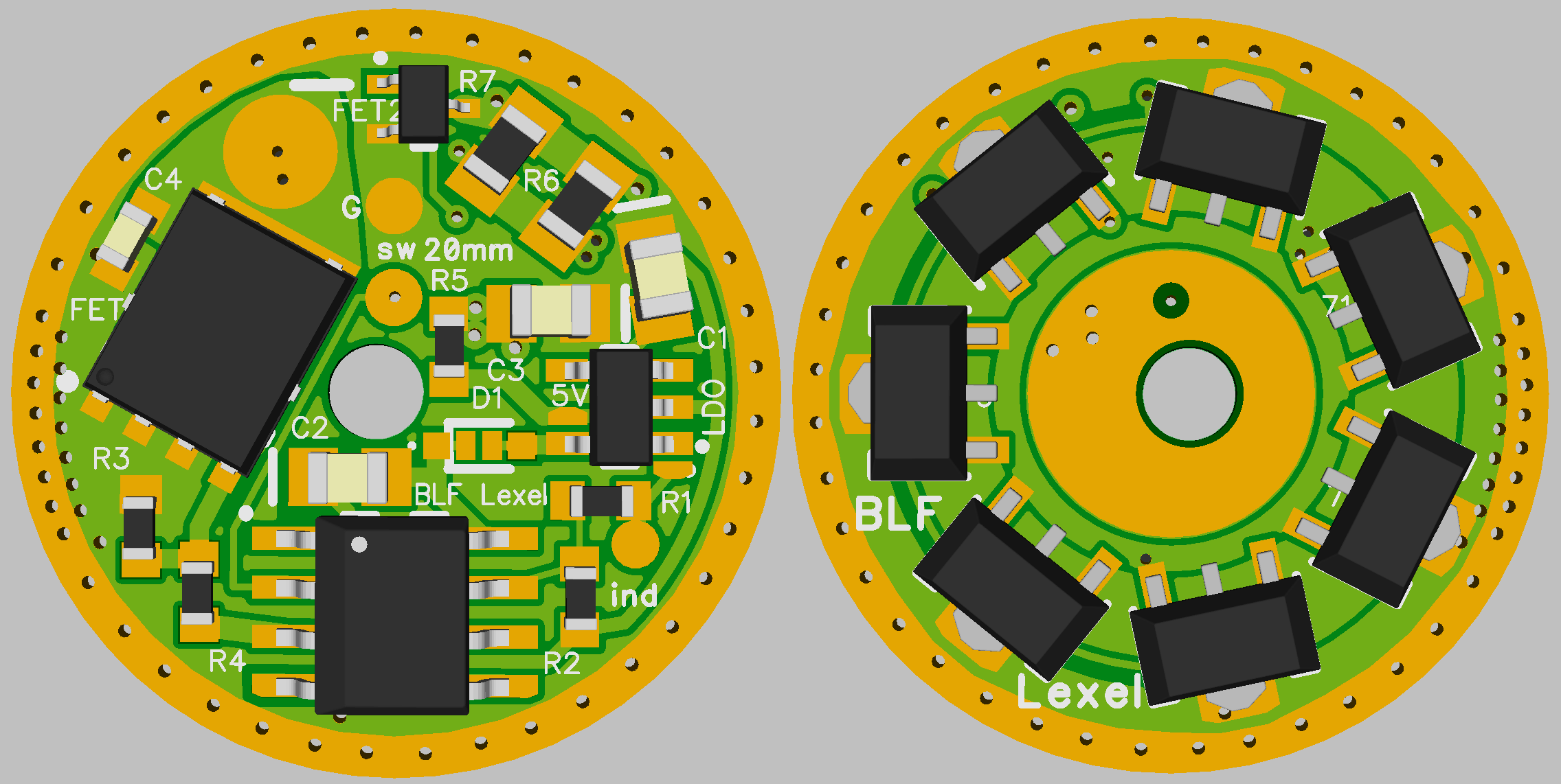
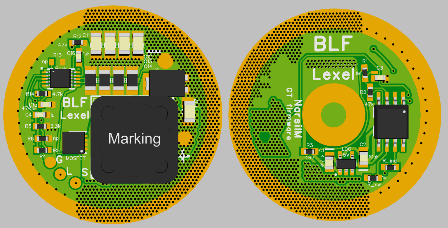
lets have a look on TA 22mm for example
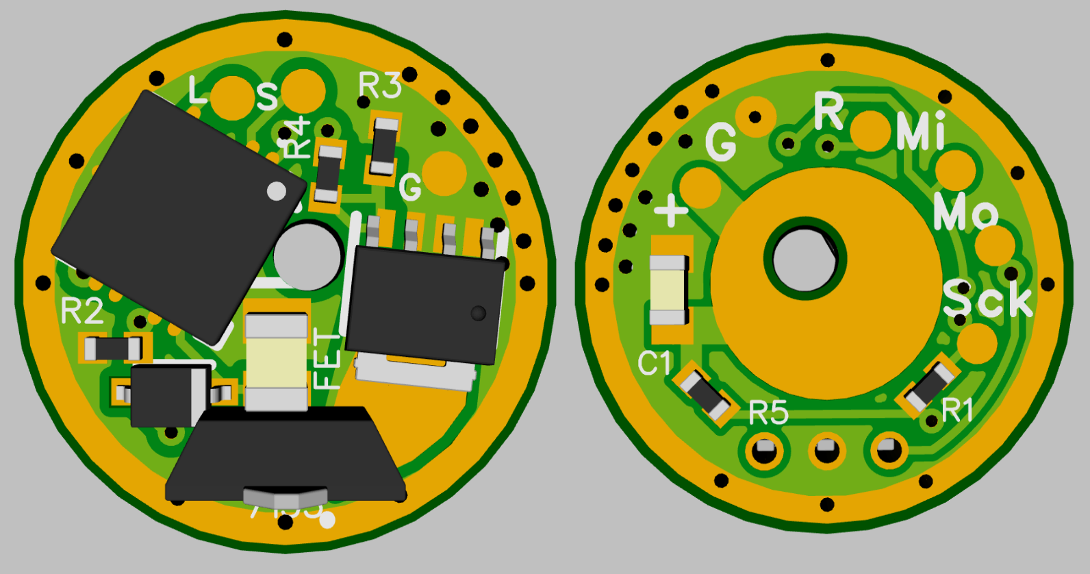
just to mention if you would solder the MOSFET this way around like seen here it would short 180° flipped
It reminds me of the layout on the Darkside Nymph driver with the 7135 chip soldered in the upright position to save space. But it isn’t exactly the same. Components are different. Yours also has (re)programming pads. Wow! Nice touch! :+1:
Can’t some of the green material near the edge be scratched off and then have a bit of solder between the driver and the body?
Like maybe near that circle at the top of the ‘G’ where there’s some free space