The Emisar D4 is a hot rod. It can run at like 80 Watts with the right combination of battery and emitters. Its “turbo” is way beyond what it could actually sustain with such small mass. It could easily damage itself or start fires.
The BLF lantern is not a hot rod. It maxes out at around 6 to 10 Watts (TBD), and it has significantly more thermal mass. It may not have a “turbo” level, but if it does, it will probably mean that the temperature goes up to 25 C below the emitter’s rated operating temperature instead of 35 C below. It could potentially get hot enough to be uncomfortable to touch, but it’s very unlikely to cause any damage.
The FET-based driver uses a linear FET design to achieve constant regulated current. It is not direct-drive. Instead, it’s like two of led4power’s constant current drivers. They’re also based on a FET.
I personally prefer the 7135 version of the driver, but it’s not because of anything related to heat or brightness. It’s mostly because the 7135 version uses fewer pins, while the FET version sacrifices or complicates some features. For example, the FET version has no pin to control the button LED, because there was no room for it.
Yes practical illumination with efficient run time for this lantern please.
Max brightness lumen monsters can be trouble… I actually got chided by a camper once, they complained that my lantern was too bright for them in the next campsite like 75-100 feet away.
(Which is also why I seconded the adjustable shield request.)
Sorry I missed that development. Previously the driver was a 7135 based design AFAIK.
It’s good to see another controllable linear driver developed from discrete components, instead of just slapping down a bunch of AMCs and PWMing them.
How well does it behave ? e.g. dynamic range, moonlight or firefly ability, etc.
A schematic diagram would be of interest, but if that’s giving away a proprietary design, at least a functional block diagram.
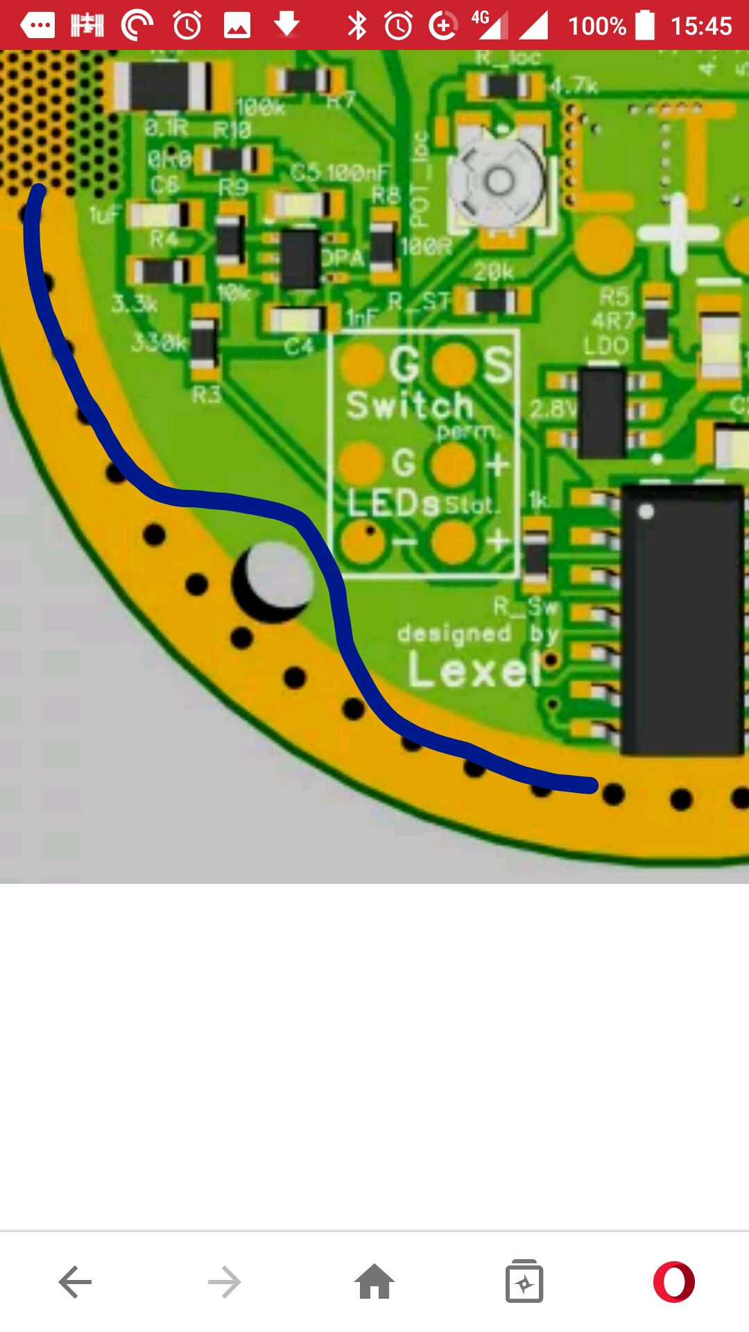
From that layout you posted, my initial reaction for Lexel is that there are far too many, and too fine, thermal vias. surrounding the FET, and the USB charge regulator. As well as being costly to produce (drill wear and time) perforating the pcb like a sieve is counter-productive and mechanically weakening. If taken to the extreme, as here, you end up with more air than copper, and I predict one small bump would be enough to fracture the PCB, given that it has to support the full mass of the cells.
Also not happy about relying on the solder resist to insulate the brass ring from the ground plane beneath it at the top, once soldered on. It might work if you specified the solder resist to tent the vias, but it’s not good practice, given the possibility of a hard short to the battery, and most good PCB manufacturers will not tent vias, for legitimate reliability concerns.
Edit: PS: there are also vias in the pads of e.g. C7 and C11, and nearly one in R18, which is usually a no-no. Particularly in this case, when if solder enters the via it will increase the chance of it penetrating to the brass ring when it is fitted.
It is stupid if that is easy to design into the lantern and does not add cost, but I would not call it stupid if it does complicate the design and costs and if tests prove that it is not needed for function.
Brass ring in latest version has also silk to cover the viases, practically the 0.3mm and 0.35mm viases will be for sure covered with 2 layers ink, there is no solder paste on the area so no risk if the bosrds have not huge silk and mask defects
We can always let in production also let them use Kapton tape for more security than that
Dynamic range with PWMing the FET OPAmps will be higher than with AMCs
Who cares if the fab has increased drill work
Even if it looks like swiss cheese those viases conduct heat much better than a simple copper plane on both sides, you see it a lot on boards with thermal load on it
I have let made MF03 board with this via density and it works, a test with MF02 with 0.3mm viases and less space between then did not fully cover with copper as it was more than 1000 per square inch, also 0.35mm viases work a lot better
also MCU with 14 pin might be an option to get all done
We do if we have to pay for it. This is Budget Light Forum Granted, I don’t know much about PCB manufacturing but that drilling certainly looks like it will add something to fabrication time. And I’m pretty sure time is money, even in China. But given how they work, if it’s a problem, they’ll just quietly remove them lol Something to watch out for.
Anyway, if it’s needed to handle the thermal load on the FETs then it’s needed. Never had any problems running FETs in linear mode myself but better safe than sorry.
You pay for area and extra services,
For example ten 10x10cm tray with 4 separate boards
4.99$ Even with 1000 drill holes
The extra services get pricey
Gold plating chemical ENIG 12$
Hatd gold 100$
Purple color 22$
4 layer 40$
0.2mm min. drill size 30$
0.1mm solder stop mask 50$
Blind/buried viases 200$
And so on
When procuring PCBs in commercial quantities the traces come for free, as long as they are within design rules.
The most costly thing about them is the number and different sizes of the drilled holes, each of which has to be done individually by the CNC machine, the maximum stack of boards, the pannelisation etc. all affect this.
This is the dominating factor when getting quotations for production (no, not small quantities of prototypes, where the setup costs dominate and details like number and different sizes of holes are less relevant and usually just ignored).
The smaller the diameter of the holes, the more costly. Those carbide drills don’t sharpen themselves
Specify thousands of 0.3mm vias, and prepare to be laughed at by production engineers.
Specify more different size holes than the machine has toolholders for, and again, prepare to be mocked.
I say again, each of these holes has to be drilled individually, one at a time, using an expensive carbide drill which might not even last one pass of a stacked panel, and if it breaks badly can potentially write-off the entire job.
And the way you have placed them, you might as well write “tear along the dotted line” on the silkscreen.
It seems to me that there has been a bit too much negativity in this thread, so I wanna say that I think this project looks incredible, and thank you to all those involved in making it a reality. Your work is very appreciated.
And it’s been said before, but to those dissatisfied with the current direction, we all look forward to seeing your alternative design.
This is looking great guys. Let me put in one more vote for USB-C PD, if it’s financially viable, it would be super awesome and make this a very modern design. Plus my phone and laptop all use USB-C so it would be mighty useful for me. But if not, that’s ok.