Being the off-time cap it’ll be ok there since you have to remove it to flash anyway. I’m glad it’s there, not that it’s hard to out it between the pin and ground but it’s always nice to have a real pad for it. Looks good, I have a light that needs a 22mm driver, I have a contact board ordered but I’d love to order a set of these for it instead and test it, if your looking for someone send me the files and I’ll order 3.
Yeah, makes fine tuning the traces a pain but make for a cleaner render (but makes your head hurt from all that tweaking, re-tweaking, and tweaking some more)
either way, once it’s done it will be a POWERHOUSE of a driver…gonna make those XM-L’s cry for mamma
This will go into a F13 and other 22mm rigs right…I got mine in today
I did mention that in post #10. There’s plenty of copper there to solder to. I’ll probably leave both pads covered in the next version and remove the mask from at least part of the two big vias. If someone wants to solder to the small 1x1mm surface area they just need to scrape.
I was confused why there is a zener diode for a single cell flashlight driver. I'm guessing you're designing in options for use in other lights later on?
Well, really just for flexibility. Mainly as you say - in case someone wants to use it in a different light. Also though, someone might choose to run the F13 on a pair of 18350. Or if some battery manufacturer ever made a good 26350 :drool:
What did I change? I don’t know. I spent too much time tweaking stuff tonight.
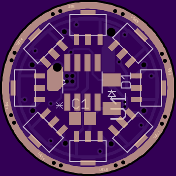
I moved the offtime cap away from the MCU. In order to move it as far as reasonably possible I had to reroute the PWM trace. The PWM trace did not have another clear path to go out of - there isn’t enough space next to the voltage monitoring trace as it is now. So I ended up having to do some funny business there in the upper left where Vcc goes onto the bottom of the PCB to get to the MCU. I seriously doubt that any clip will be able to grab the MCU, but this should make messing with the MCU easier.
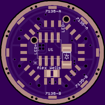
I reduced the annular rings on the vias to improve clearances next to the big 1.1mm LED+/- vias. I re-covered both solder pours with mask and uncovered the +/- vias.
I labeled everything I wanted to - I do realize that the zener only has a zener symbol and the offtime cap is unmarked.
I marked two sets of 7135’s: “A” and “B”. You must place a 7135 or jumper to GND with at least one location from each set. Each set has 4x 7135’s in it, two on top and two on bottom. It should be really easy to make sure at least one from each set is populated.
I realized that there was no reason for the exposed copper GND ring on the bottom of the board in this application, and it’s actually a pain because it prevents you from easily aligning the 7135’s. So I put the mask back over that and removed the mask from the vias because I think that looks cool and why would I need a better reason than that I also realized that I do not have a polarity marking for D1. Oops. Hopefully that gets fixed in a future revision. Maybe I’ll feed the voltage divider directly from BAT+ in a future revision too.