I haven't noticed them making heat, but I haven't specifically checked them for that, either. The only part I noticed trying to burn my fingers was the big diode down at LED+. These are just limiting resistors. I could swap the resistor locations around, and change the mode order.
This must be the section handling the low mode, since the other 3 are already known:
The little 180 (or 18C?) is the limiter, or the 010? What's a '010' anyway? My go-to decoder page says it's not a valid marking. Through that 010, there's a direct path to the #3/FB pin at all times. I haven't tried, but I'd assume that shorting the 010 resistor there would affect all modes, unlike the other 3 resistors that all work independently (in mid, shorting the H or T resistor has no effect; in high, shorting M or T has no effect, etc.).
Resistors like R120 and R500 are definitely sense resistors, not limiting resistors.
You may be able to directly measure the resistance of those two resistors you’ve got in the red box. What does that show? I’d measure both directions on each. I’m not sure how the transistor (or whatever) & capacitor there affect the operation of that section.
Basically the whole board could be “low mode stuff” since low mode is just a baseline and all the other modes are higher. Almost any of the small components could be involved with setting the baseline current and voltage… But yeah, that section is a suspect.
Your latest pictures show that there should be a break in the green line in your colored-in pic. Each of the sense resistors connects (through a dedicated transistor) to the big copper pour on the back which attaches to the FETs.
Due to the camera orientation, I cannot see where the via between the big cap and the red box you drew connects.
Immediately to the left of your red box there is a via, this appears to head down to the diode marked XL, through a resistor, and then on to Vin (Pin 9). I don’t think that’s what’s really happening, that’s just what I see.
Personally I am much less interested in this driver board now that I realize that it does not use a dedicated LED controller. It is very complicated for what it achieves.
FWIW, the FB pin is for setting voltage, SENSE pin is for setting current. I think.
If they are sense resistors, which component on the board is reading their voltage drop? If the LTC1871 were controlling the modes I could see it, but we know it's not. It looks to me like it just boosts up to whatever set point, then the path to ground is routed through the appropriate resistor via each mode's little FET.
The big cap between the inductor & the LTC1871 is on the main B+ pad on the R/H side, its L/H side goes to a longish fat trace that goes down to a medium size cap, the thing marked 82LE, and a tiny cap. There's a big horizontal B+ trace at the top of the inductor. Easiest seen in this pic:
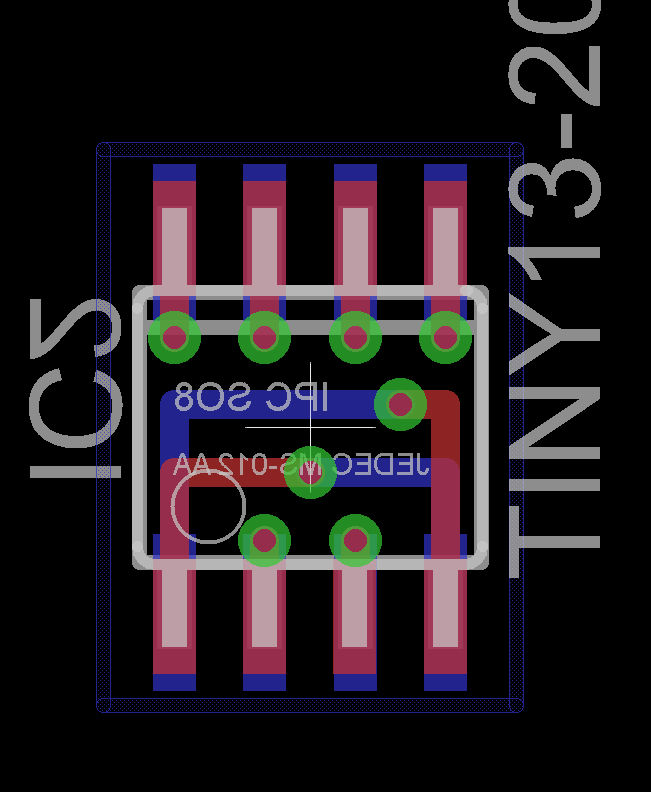
Anyway, I'm about certain there's not enough room in the light to fit a piggyback board on top to hold the attiny - depth in the head is only 5.8mm off the top surface of the original driver, and the inductor takes up 3mm of that already. The only workaround I can think of at the moment is something like gluing the attiny upside-down onto the board where the original MCU is and use jumper wires to route the legs to the right pads. :(
Funny you should mention that. I worked on this some but decided it was a stupid idea. You have to reflow the adapter PCB onto the main PCB of course - either a big hoof tip or some chipquick might do OK, or just hot air. Then you solder your regular ATtiny on top. Total height should be around 3.5mm
My bad on sense-vs-limit. Now that I think about it I’m not certain that they aren’t limiting resistors. At this point I could go either way, without a schematic it’s hard to guess. Gotta figure out what’s hooked up to the SENSE pin to know for sure. This thing can do a weird sensing setup as well as a more normal one. I’m not certain they aren’t used for sensing, but I’m leaning towards you being correct.
Thanks for the clarification on that path, I see it now. The LH side of that cap is a ground of some type, even if it’s not real GND. The medium sized cap you mentioned hooks up to INTVcc (pin8), so it must be a smoothing cap for that. (Therefore the other side, which connects to the big cap, is ground).
Is the mode separation as good with the MT-G2 as it is with a triple?
Just from memory, I think the output currents were something like just a few mA in low, .25A in M, 1A in H, and 1.5A turbo. Of course now we know what they do, those levels can be adjusted with different resistors. I don't know how that compares to when it's running the 3S XPG2s, though.
Sorry, now I forgot what I planned to learn from that.
Anyway I went ahead and put an outline on that adapter PCB and uploaded it to Oshpark. It has to be slightly large in order to meet minimum size restrictions, you can file it down.
~~http://oshpark.com/shared_projects/WtKCjCqt~~ EDIT: see post #57
I also thought about putting a via through the middle of each pin. You’d need to file up to halfway through the via, but it would make the board easier to hand solder.
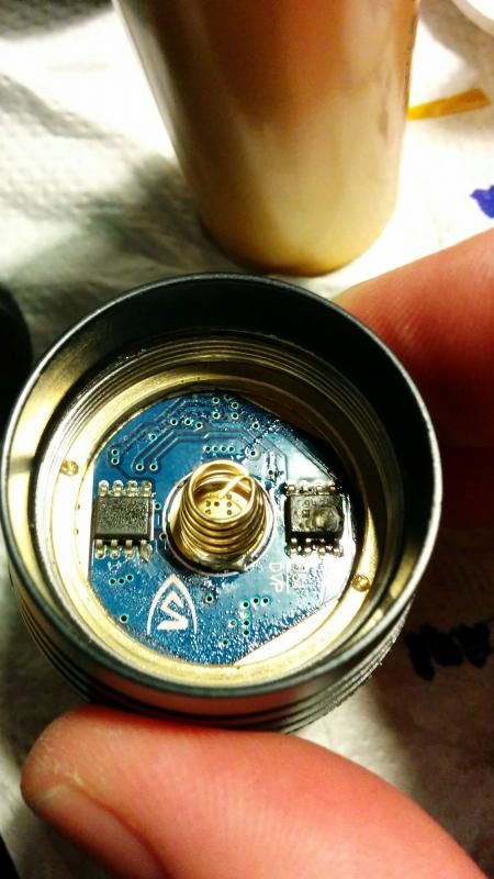
just burnt my driver, bridging the r120.
one of the two mcus, that they are on the spring side, burnt.
If I try to power again the flashlight, this mcu burns again.
I measured 11 amps on high with a KK 26650.
Those are FET’s, not MCU’s. They are just in the SO8 package.
I only know the model information for one of those two. It seems you are lucky, you burned the one we know about.
We don't really understand how this driver works. Swapping FETs could cause big problems. That said, maybe a PowerPAK SO8 style FET would be a good choice. For example, the SIR462DP can handle more current and has much lower RDS(on) figures than the stock FET. You'd have to take a look at what is under the FET and make sure that you weren't bridging anything. I wouldn't do it.
AO4468 is also used on other drivers, most common one is probably the 3-toroid SRK drivers. If you have any dead drivers laying around it's worth a look.
edit: Also, I doubt there is any other FET out there that will survive having the resistor bridged. Being a boost driver, the input current isn't self-limited by the LED voltage like in a DD setup, and that's why these same parts survive fine in other driver designs but not in this one.
My comments on replacing the FET were not intended to facilitate bridging the resistor, just decreasing the resistance. It’s still not a great idea either way, as I mentioned.
I got confused when making these adapters. Do not use them, they are clearly wired wrong. I knew better than to do this and did it anyway - oops. I’ll re-attack the problem and get it right next time.
OK, v04 -> v06. Now the adapters should be functional, but after that last mistake I wouldn’t trust me if I were you.
I didn’t bother to keep track of what order the pins are in now compared to where I thought they were with the previous version of this adapter. They are in the order that was easiest for me to route while still making GND and VCC connections. So the firmware I posted above (and never tested of course ) may need some tweaks to work with this board. Pins 2, 3, 5, 6, & 7 are all straight through. Pin #1 on the ATtiny (PB5) goes to the location of Pin #4 on the PIC (GP3).
I think there is no interest in running STAR on this light using the stock levels, but for the record I think the latest firmware I posted has an error. It looks like I forgot to set “RUN_PIN” to output along with the MODE_X pins.
I have replaced the mosfet but I noticed that the sprint of the driver gets really hot after some seconds of running. I worry that might some other components have damaged, except the replaced mosfet. Using a fet driver with star firmware is my next step, what do you think?