You certainly know how to attract flies modders. I like this idea, the benefits of regulated output plus the overdrive of FET DD. Now you just need some programmer honey.
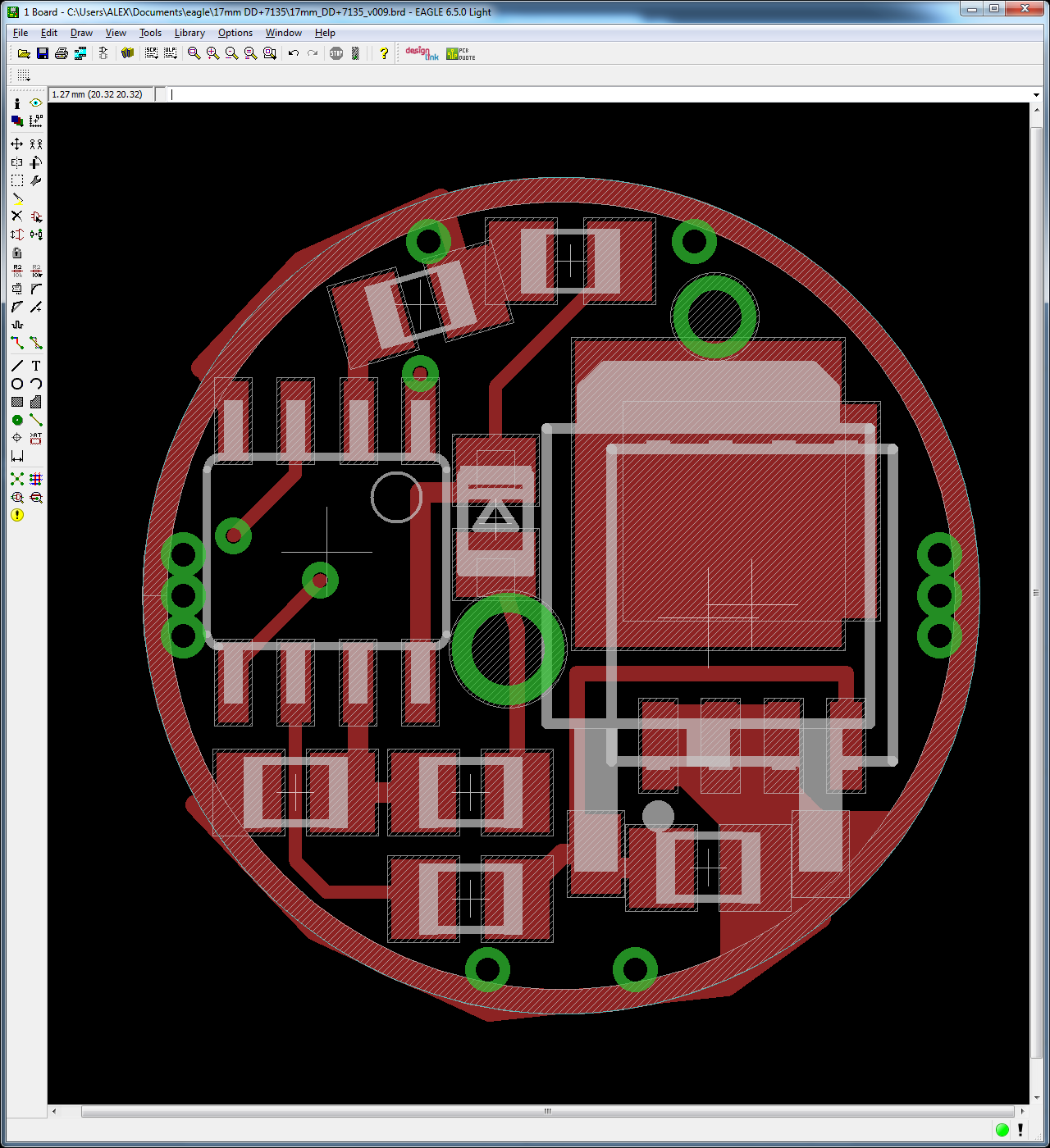
Texaspyro will frag your A$$ for running the signal trace under the AMC chips. Is it possible to shrink the center pad to allow the trace to run inside the chips?
Not if you want to solder a spring to it…it looks like a full 5mm pad that has some solder stop over it…any smaller and good luck even soldering a flipped over spring to it, 5mm is teeny tiny
Why? As far as I can see they both fit, it just looks unattractive. This way nobody gets caught with a board/FET pair that don’t work together and has to wait weeks for Oshpark to send a new board.
The pour is 6mm, the exposed contact is 5mm.
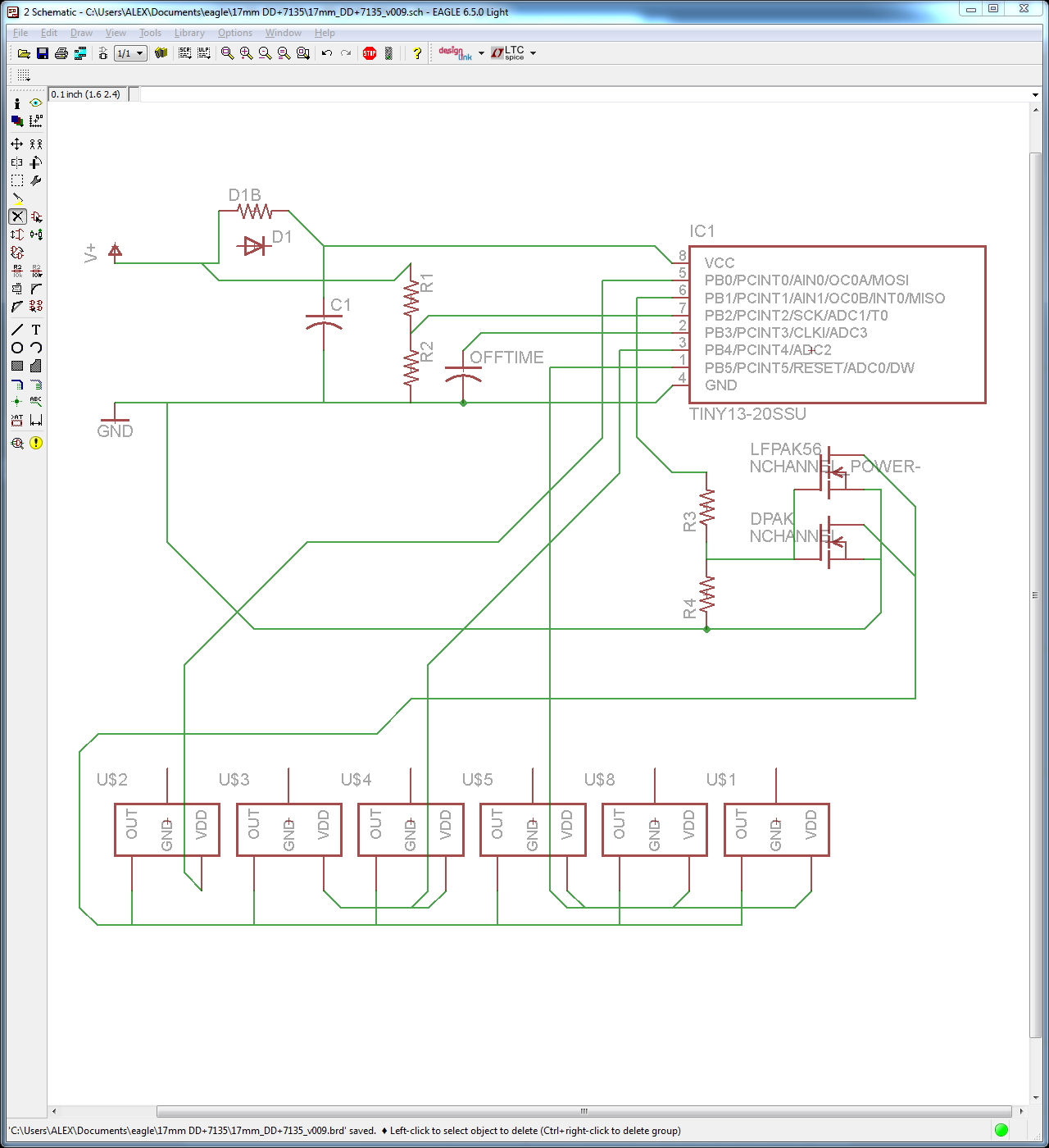
It uses 4 output pins for that. PB1 is PWM, that is hooked up to the FET. I should swap PB0 and PB4 so that the single 1*7135 is also on a PWM pin (PB0).
It works the other way too. I figure it’s easier to solder a 0603 on a 0805 pad than the other way around. Soldering 0805 on a 0603 is a minor pain in my butt. Thoughts?
When the time comes I want 8k or more. 8k will hold a bootloader for programming without ICSP. You should be able to program a chip which has a bootloader using 3 wires or less. Header time! Unfortunately the ATtiny85 is probably the best candidate for that and in SOIC it’s only available in 208mil package, not the 150mil we use now. It won’t fit on boards like this one. The MLF package (20M1) is an option, but you can’t bring vias up under it and pass them over to pins like I did on this board. Also realistically it’s reflow only.
Good suggestion. I was being lazy because I do not enjoy working on parts. I should make a new part that eliminates that pin and the stop. That will make it much easier to route in a semi-attractive manner. The trace still may end up under the pin. As long as you don’t have much chance of exposed copper (like a tented via that gets solder down inside it) I think it’s OK to route the trace under there.
Might help the - via by putting some top copper at angles to the FET pad just to smooth out the bump so to speak, and provide a little more copper for current flow
I can see advantages to both ideas. You have a point about versatility with the current superimposed FET layouts wight but an lfpak56 only design would give the board a bunch of extra space on the mcu side. I love a challenge so bring it on.
I took RBD’s suggestion and deleted the middle pin on the 7135’s. (and I cleaned up the traces on the bottom) Remember, the pins are still there just with no exposed copper under them.
WarHawk-AVG - I doubt that current handling will change but I will add copper around the via as an aesthetic touch.
I moved the solo 7135 onto PB0. The firmware should be able to put PWM on either the FET or the single 7135. With a single 7135 you can probably get moonlight low enough and still be regulated… I’m too lazy to try it.
It seems almost certain that a driver with one chip with a low pwm input will be capable of a lower moon mode than a driver with 8 chips at the same value. This made me think of WarHawks test board for 7135’s. By hooking that board up to a driver set to moon mode it should be possible to test various 7135’s to sort them by their low level output. They’re fixed and pretty uniform at full but not nearly as uniform at low levels. Now I have to find that thread again. Where is it? I saw it under the chair a minute ago.
Your wish is my command. For this driver and others that use multiple output pins I was thinking of using arrays for mode storage. Maybe a 2-dimensional array could hold all the modes and all the PWM settings at the same time. I think that might eat up a lot of memory though, I haven’t tried it.
Good question! No firmware updates from me, I haven’t done anything useful.
I started to do something productive (not related to firmware) earlier today and then caught myself and fired up Eagle instead ;-). I’ve decided that RBD is right, the DPAK sized FET is a waste of space. The board now requires a Power-SO8 (LFPAK) sized FET. This shouldn’t incur any cost or performance penalty, so “it’s all gravy” as they say.
I’ve implemented the [June/July 2014] anti-boost fix for the DD drivers (eg I moved the decoupling cap electrically to the other side of the diode). I removed the resistors previously present which were related to driving the FET properly, IIRC they aren’t necessary for this after moving the cap.
Between those two changes the top of the board is looking a lot less hateful for anyone who has to solder this by hand. I think it looks completely doable now.
As usual note that there is no firmware so this hardware is just for firmware developers and masochists.