DEL - that dang little cap across the MCU worked !! At least so far. Before on a SANYO GA strobe didn't work at all, and now it's working flawlessly so far. Accept the dang thing gets so hot so quick. I'm using 22 AWG LED wires, added spring bypass's on the tail spring and in a tiny driver spring I added - original driver had no spring at all.
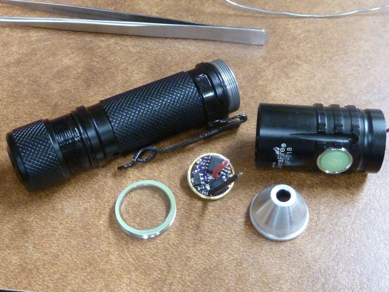
A pic of the UF-T18:
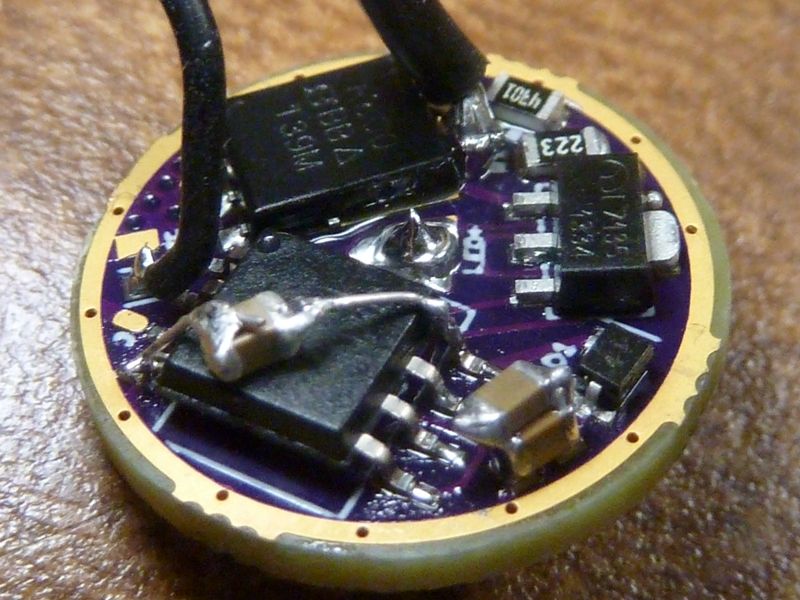
Here's the driver in it's final/current version:
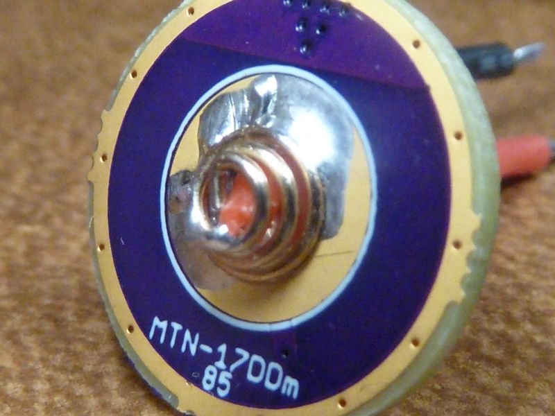
Here's the driver spring w/bypass (used a 26 mm wire in there - very short):
At the tail, I got 6.3A with the GA cell - crazy #'s, but with the 219C 5000K, I'm getting about 1,000 lumens out.
Note: Both added caps above are 0.1's, but, one is 50v rated (square on the MCU), and the thinner one must be a lower V rating, but not sure what it is.
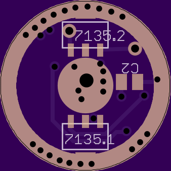
I'm thinking we need a board design with a 0806 pad for a cap that gets + after the diode, close to the Vcc MCU pin #8, and either goes to a strong grnd, or gets to a ground close to the grnd MCU pin #4.
I dunno how it would fit on a 17mm board with the wide pads for a 45/85, but, thinking this will be the ultimate solution - using a 0.1 uF cap, or thereabouts.
I also would love to have pin #3, the spare I/O pin wired to a pad for a secondary switch, or ON/OFF LED output. I think the MCU pin #3 can work for that.
FWIW, I finally merged in Tom E’s eswBrOutCfg project.
Also, I’m still eager to hear about further developments on the issues you see on strobes and other sudden flashes. The cap over the MCU is interesting; I wonder if it could be placed somewhere directly on the board or if perhaps some other solution might work better.
Now I’m really confused. I think I’ve dropped the ball on this topic…
Wasn’t the conclusion that the cap should get + before the diode? Or are you considering one before and another after? Don’t most of the drivers have the cap + after the diode?
If space was an issue, the board could use the SSU footprint and the cap be placed under the MCU. It would require the SU MCU package to be used and the pins to be bent in. When this is done, the MCU sits high enough to clear small 0805 caps underneath. Bent legs really make program clipping much easier.
Mike - yes. The large cap should remain before the diode, small cap after, at least that's what it's looking like. Think it gives us best of both. The test light continues to run smoothly. I got 3 lights now that had the problems and fixed now, all slightly different in cap values and placement, but all have a high value and low value cap, and the low value is after the diode.
The last driver, RMM's, is using a 0.1 uF cap, not 1.0 - DEL recommended the 0.1, though might not make much of a difference (I think).
Edit: that may be a viable option bout the bent pins technique. I am a bit concerned though bout the soldering of the MCU pins - certainly not as robust as when they lay flat on the pads, normally. I've done a few though and plan on doing more, and seems to be holding up well, but usually have to touch up a pin or 2 by hand after reflowing.
I vote for under the MCU.
It can even be on the opposite side of the PCB, but that would spoil the ‘single-sided’ feature. Vias also decrease decoupling performance somewhat.
The go-to size for local decoupling is 0.1 uF, but I think 1 uF will be fine as well in this case.
The tracks connecting pins 1 and 8 to this cap should be as short as possible and around 50 mils wide.
Atmel’s recommended decoupling is more concerned with noise emission from the MCU, but describes the basics well.
Atmel also recommends a series ferrite bead, this is not that applicable to our single supply MCU’s.
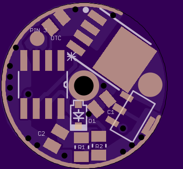
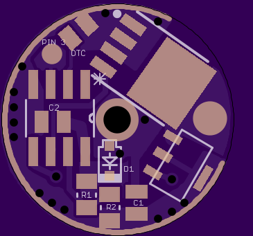
I’ve made a start and added a few extra features very difficult to get everything to fit.
Pin 3 has a 0.8mm via that leads to a 7135 that can be populated if wanted or the via can be used as switch in ect…
The pads to the right of the MCU are the extra cap. It could be moved to the opposite side later.
Don’t think I will be able to get the 85v foot print, but I’ll work on it more later.
DEL could answer this better, but I'd say probably not. This is more or less for us hackers , but, the chinese changed the BLF A6 driver anyway, so they did not 100% duplicate the wight FET+1 driver we started with. The soldering problems were not a design issue - it was a manufacturing/production/QC issue - sloppy and rushed basically, from the looks of it.
I work for a manufacturing company, and we insist our PCB suppliers test the boards before shipped to us. We will design/engineer/produce test fixtures for them to use in order to achieve as close to 0% DOA failure rate as possible. This is one way of doing QC - you want this done as close to the source as possible.
Sorry to say the way our group buys are done here are far from ideal in time and cost. This whole cycle of sample testing in the US is very inefficient and wasteful, but not much other choices unfortunately...
Let me verify the clearance under an 85 with bent pins tonight. I'm pretty sure that there is height for a 0805 1uF, but I haven't tested that idea yet.
Think it will depend on the voltage rating as well - higher the voltage, bigger the part. Think we use 16v rated caps in general. I believe it helps having a higher rating - not sure.
Gap under an 85 with legs pushed in most of the way to touching the chip is .028" to .029" (.72mm). My 1uF caps in an 0805 package (I believe 16V rated) measure .034" to .035" (.88mm). So it seems one could get away with a cap under the MCU as solder can quite easily bridge a .006" gap.
Or, the gap could be completely eliminated by slightly straightening the legs.
I've been away from this game for far too long; it's time to jump back in again. I had to force myself away just when things were getting interesting around here so that I could focus on some of my "other work".
The layout on that 85 driver I did really stinks...way too much space around the MCU, but I figured that it would be easy to flash the thing a million times. It looks like it also needed a bodge capacitor to work right. I guess I should have labeled it "alpha".
I haven't read through everything here, but a capacitor underneath the MCU sounds like a really bad idea unless you like tedious leg bending and soldering on every driver. I'm sure we can make it work without resorting to stuff like that.


 , but, the chinese changed the BLF A6 driver anyway, so they did not 100% duplicate the wight FET+1 driver we started with. The soldering problems were not a design issue - it was a manufacturing/production/QC issue - sloppy and rushed basically, from the looks of it.
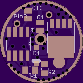
 I had to force myself away just when things were getting interesting around here so that I could focus on some of my "other work".