The basic circuit follows the one BLF SRK FET v2 by RMM is using. I deliberately designed v3 to only add functions and kept all that was already there, including 2S support with LDO, OTC, Temperature Probing, Switch Pads for Pin 2 and 3, Gate and Pulldown Resistors, Star Solderpads, 5 LED Wire Pads.
You find a detailed partlist when you follow the link to v2, so in the following I stick to the changes and additions.
FET
LFPAK56 instead of D2PAK package
Channels
There are now 3 channels for current regulation
The single AMC7135 (Q1)
The FET
Up to 9 AMC7135 (Q2-10)
Pin5 of the MCU is hardwired to Q1.
Pin6 can be connected to the FET or to Q2-10
Pin3 can be connected to the FET or to Q2-10 as well
The selection is done with the 4-pad-connector:
Bridge the pads vertically to connect the FET to Pin3 and Q2-10 to Pin6 (like I did above)
Bridge the pads horizontally to connect the FET to Pin6 and Q2-10 to Pin3
Capacitors C1/C2 (for MCU, LDO)
I redubbed CLDO as C2
In 2S configuration with LDO you need both capacitors
Momentary Switch
Connect one cable of the switch to SW- (=GND) and the other cable either to SW(2) or SW(3), depending on whether the firmware uses Pin2 or Pin3 of the MCU (Pin2 is commonly used)
Well this looks very nice.
I am with MRsDNF that most is not directly understood by me (and that this is my fault)
I think it looks nice enough to be used for that special BLF watch Kronological was working on, besides just put it away from sight in a SRK
To be fair my inspiration for triple channel stems from @wight and his long retired A17-Hybrid driver. We owe him a lot.
But, having said this…
Same to you, PD. If it wasn’t for you, triple channel might never have come out of its niche. So thanks for taking the time to develop and publish your drivers, I know how much work it takes.
Admittedly I stopped following TripleDown when it went to Bistro / Narsil, so I can’t say at one glance whether this v3 driver is compatible to TripleDown or not. I still stick to the good ol’ 13A. It was so time-consuming for me to understand its functions and to adapt the firmware, that I don’t muster the time to add another MCU to my portfolio, yet.
I haven’t left the the 13a either. There are very different versions of the TripleDown with different purposes, your “quad pad” thing accomplishes most of the differences. The firmwares should be mostly compatible, just without the other goodies you added
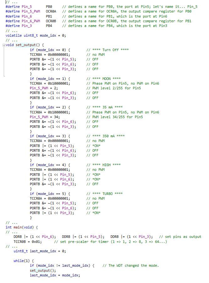
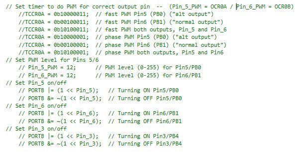
Well, errr, it’s nothing but an adapted version of JohnnyC’s Star Momentary, made for ATtiny13A, and very clumsily set up (simple if mode_idx==…, then…), embarassingly without good commentary, as I always change the code and don’t adapt the… commentary.
- sigh -
I’ll see what I can do.
.
Good to know. I’ll need to take a closer look.
Oh, and the “goodies” are not mine. It was RMM who added all the fancy stuff in BLF SRK FET v2, I just left it in the design.
Thanks, if you get github up and running I would like to download the whole .c if this is possible. I try to get a tripledown driver to work in a dual switch light. But the e-switch does not change modes so I’m a little stuck at the moment and thought maybe your firmware would work with the tripledown driver and e-switch.
Nice Job on this! There's sooo many pad/options, trying to trace them is mak'n my head spin! But I see how a lot of it is working.
I also see you are using a FET gate pulldown, 33K, but not using an Rgate resistor - did you find it necessary? I've used anywhere from 12K to 47K for the pulldown, but we assume can go up to 60K or so. I've settled for 47K for now on the BLF Q8 driver, but haven't scoped it. For the Rgate, we are using a 100 ohm, and I see Richard recommends a 10-50 ohm.
Yes, RMM recommends 20-50 Ohm for the gate resistor, but he kept quiet about the pulldown resistor. I don’t have a scope so I just kept reading what these R are for and how their value should be. This is not as easy as it looks, as both are often referred to as “gate resistor”. And the funniest calculation was this, which the author deemed as minimum knowledge needed about gate circuit resistance in MOSFETs. Well, he lost me at point 1…
So this was my train of thought:
Although frequency does not really matter in my design (no PWM), spikes will in all probability occur at switching. Now I’m not sure which of the two R prevent that, so my intention is to use both.
The pulldown resistor is said to be necessary to keep the gate from floating. Values between 1k, 10k and 100k ought to work. BLFers had good testing and scope results in the tens of kOhm, so I used the nearest I had which was 33kOhm.
The (series) gate resistor shall protect the output pin of the MCU by preventing overcurrent. There’s talk of values between 10 and 150 Ohm. I have no such value at hand… Well, the Attinys are said to have overcurrent protection although I couldn’t confirm it. But a lot of BLF FET driver were built without a gate resistor, so I dared to build it with a 0-Ohm-resistor for now. But I plan to use a gate resistor after my next parts order, because it might help preventing spikes, might protect the MCU and will not hurt the output. I thought of 50 Ohm, but I’m open to suggestions.
.
Err, another thing, while we’re talking resistors… R1 and R2 (LVP).
How high can we go to
- keep parasitic drain as low as possible
while still get reliable voltage measuring from the MCU?
With my values of 33k/8k2 (I still prefer behind D1) I measure a parasitic drain at sleep_mode of 0.25mA. Now you use (before D1) 220k/47k for ages and probably with good measuring. One might think of even higher values, like 2M2/470k, 22M/4M7. Is there a limit where the MCU will not be able to measure the voltage anymore? Could that be calculated?
Can't recall, maybe Mike C tried higher values for R1 and R2 - he said what those were, can't recall - hgiher than my 10X though and pretty sure proven to work fine. I used 10X factor because I had them, common sizes. But I also bought limited qty of values bout 3X higher than that, effective cutting the R1/R2 drain by another factor of 3 -- didn't try this yet. Dunno if there is a theoretical limit on the values, but 1M or 2M for R1 sounds familiar think it was tried and worked.
The 13A is well proven to tolerate spikes better than the 25/45/85, so, these gate resistors are probably not needed at all on a 13A, but on the scope, things look much better with them.
More important for reducing parasitic drain than tweaking higher R1/R2 is making a correction in the firmware to shut down the AtoD when goin in sleep mode - forgot the difference but it's big. First recommended by Halo in the 24/45/85 thread - dunno, others might have done this in custom firmware but as far as I know, none of the standard open source versions do it.
I'm seeing 0.007 - 0.009 mA drain in a few stock better lights, so it's done and out there. For me, I just think no one should have a concern about draining the battery simply because it's left in an e-switch flashlight vs. a power switch light.
I’ll change R1/R2 from 33k/8k2 to 330k/82k first, just to see the practical result. In theory it should lower the parasitic drain (@4V) about 0.09mA, pushing it from 0.25mA to 0.16mA. I might try another x10, which would save another 0.009mA, and see if voltage measuring will still work.