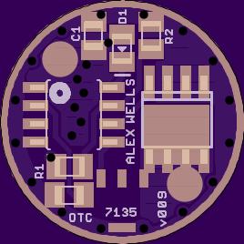
I’ve worked on this before and the layout did not work decently. In the past I depended too heavily on the LFPAK outline I grabbed from the internet. When I saw RMM take a crack at the problem (#3441) the truth is I initially dismissed his work: I thought to myself “shows what he knows, that stuff won’t fit.” Later the idea kept rattling around in my head again and it occurred to me that both RMM and I have built the A17DD-SO8 drivers and know exactly how much space each component needs. Clearly I needed to reconsider. Knowing how large the actual components are once installed on a driver like this makes a difference (as one might imagine :p).
Features:
~1.0mm ‘tall’ component keepout around edge. (7135 tab extends to no closer than 0.5mm of the edge.)
FET + 1*7135: alt PWM is hooked up to the single 7135 so it may be possible to get this working with an unmodified version of STAR.
No Zener! Sorry MT-G2 folks, you’ll have to stack a Zener across C1 or between D1 and R2. Or maybe kind of wedge it between R2 and the FET.
Offtime ready.
Large 1.5mm GND ring on bottom and on top (where possible). Exposed copper is 0.5mm on top and bottom.
Like some other recent drivers, this driver does have a reverse-polarity protection diode but bypasses the diode for the voltage divider. Due to this we are able to use any diode desired. Ideally we use a protection diode with as low a Vf as is reasonable.
The exposed spring pad is 10mm. Total pour diameter is 12mm.
LED +/- pads are 2.5mm in diameter. They’re on much larger pours and diagonally across from one another.
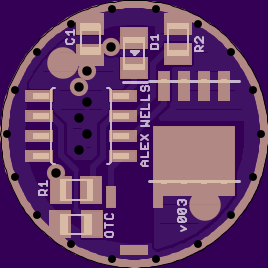
I’ve worked on this before and the layout did not work decently. In the past I depended too heavily on the LFPAK outline I grabbed from the internet. When I saw RMM take a crack at the problem (#3441) the truth is I initially dismissed his work: I thought to myself “shows what he knows, that stuff won’t fit.” Later the idea kept rattling around in my head again and it occurred to me that both RMM and I have built the A17DD-SO8 drivers and know exactly how much space each component needs. Clearly I needed to reconsider. Knowing how large the actual components are once installed on a driver like this makes a difference (as one might imagine :p).
Features:
0.5mm component keepout around edge. I may trim this up to a larger number in future revisions…
FET + 1*7135: alt PWM is hooked up to the single 7135 so it may be possible to get this working with an unmodified version of STAR.
No Zener! Sorry MT-G2 folks, you’ll have to stack a Zener across C1 or between D1 and R2. Or maybe kind of wedge it between R2 and the FET.
Offtime ready.
Large 1.5mm GND ring on bottom and on top (where possible). Exposed copper is 0.5mm on top and bottom.
Like some other recent drivers, this driver does have a reverse-polarity protection diode but bypasses the diode for the voltage divider. Due to this we are able to use any diode desired. Ideally we use a protection diode with as low a Vf as is reasonable.
The exposed spring pad is 10mm. Total pour diameter is 12mm.
LED +/- pads are 2.0mm in diameter. They’re on much larger pours and diagonally across from one another.
It looks fine to me. I’d have no qualms about ordering the PCBs if I were you. It’s possible that I’ll continue to make some minor tweaks, but the design looks good in Eagle and on the OSH Park previews.
As far as I’m concerned it’s a WIP until at least one revision is actually assembled and working.
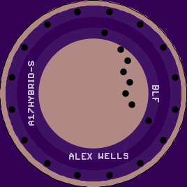
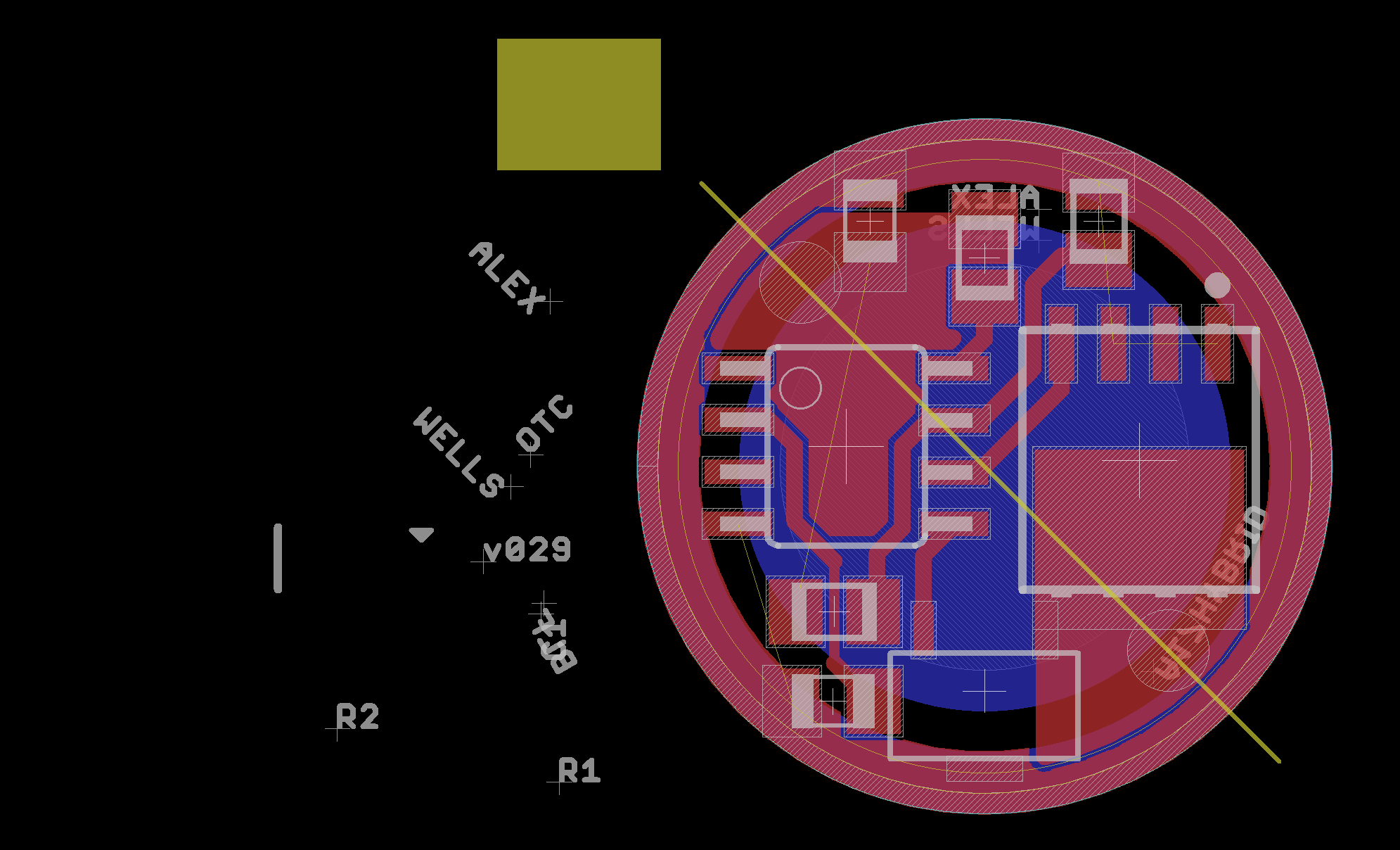
I forgot to mention that those vias are extremely close the the edge of the board. If there was a problem, that’s where I’d expect it to be. That’s something I expect to tweak. I don’t think that OSH Park will fail to plate the vias, but the GND vias do not meet OSH Park’s design rules. Assuming that the vias are drilled and plated this could result in only partial plating of the through-hole itself. It will certainly result in the vias not being entirely surrounded by copper on at least one side of the PCB (the bottom side). I expect the line to cut directly through the middle of the vias. What I expect is to see something like what led4power gets over here (but slightly worse): FS: LD-1 driver (5Amp pwm-less linear)-SOLD
Wight, for whatever reason the board outline doesn’t line up with the components when uploaded to OSHStencils.com. Really doesn’t matter as the actual cut out’s will be aligned with the pads to use it, just thought you’d like to know something is off somewhere.
Very nice wight, feels very balanced with the max POWAH and battery saving lows, i can’t wait to see someone build it,
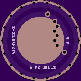
Would these work just like a A17DD-SO8 if the 7135 pad is not populated?
It would be very interesting to see a comparison on run times for the FET on low from a A17DD-SO8 and this one.
If you’re going for truly low then the range of battery voltage from fresh to empty is an issue. PWM levels which barely light an LED on a full cell (~4v) will not light an LED with an empty cell (3.0v to 3.5v). The 7135 should help with that.
Thanks WarHawk-AVG! I’m not sure that we can’t do better. I’d love to see it get a little more symetrical if possible and shrink a little tiny bit so that the GND ring vias can move inward.
Thanks cajampa! Again, the actually cramming all of this onto one PCB wasn’t something that I thought could be done before I watched RMM do it.
Yes, these will function like an A17DD-SO8 unless you do something to make use of the extra hardware.
We’ve seen this before, it’s not really clear to me why it happens. I did change CAM jobs, but I don’t know whether that is related. If I remember maybe we’ll try a different CAM and see if it does the same thing.