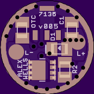
This is a two-sided driver intended for use with DD 10440 lights. It is based on the same schematic used for the recent 15mm and 17mm single sided versions. It makes use of an LFPAK33 or other similar MOSFET in tandem with a single 7135 for lower modes. It is intended for use with the Dual-PWM feature in JonnyC’s line of STAR firmwares.
Features:
Extra unattractive appearance. Hard to do much about that. This is a tight squeeze!
~1.0mm ‘tall’ component keepout around edge. (7135 tab extends to no closer than 0.5mm of the edge.)
1mm electrical keepout around the edge.
FET + 1*7135: alt PWM is hooked up to the single 7135
Full solder dam for the 7135’s tab - makes assembling this small driver easier.
3.3x3.3 sized MOSFET, recommend LFPAK33 because it has exposed leads.
Offtime ready.
Large 1.5mm GND ring on top, 1.0mm onbottom (where possible). Exposed copper is 0.7mm on top and bottom.
Like some other recent drivers, this driver does have a reverse-polarity protection diode but bypasses the diode for the voltage divider. Due to this we are able to use any diode desired. Ideally we use a protection diode with as low a Vf as is reasonable.
NO EXPOSED SPRING PAD. This driver requires a BAT+ strap across the ATtiny13A.
LED +/- pads are 2.0mm in diameter. They are positioned precisely across from each other.
Notes:
A very careful install of the strap should allow the programming clip to fit.
This driver should sand down to 11mm without issue. 10mm is too much.
LED +/- pads are 2.0mm in diameter. They are positioned almost exactly across from each other (within a 0.1mm tolerance of exactly across from each other).
Even better do you have an estimate on how thick this would be assembled? and you didn’t say anything about shaving on this one like the 15mm single sided, is it possible to shave this one to 11mm?
I still dream about a single sided dd fet driver with one of these modern tiny FETs in 10-11mm, is something like that even remotely possible? maybe if you use the smallest smd’s like the 0603,0402,0201 or crazy tiny 01005.
Edit
You are developing drivers so fast you didn’t have time to add this one to your signature
I wish the post office, the slow china holiday mail and my modding skills would move as fast as you are developing new drivers i may newer get a chance to try them all, i think this will be an interesting 2015 :party:
Nice, another great addition to the Alex Wells driver family.
One recommendation: to make that batt+ strap you really want an extra batt+ solder pad on the other side of the MCU, just a dummy pad going nowhere (there's room for it, it seems) so that you can solder a wire over the top of the MCU and fix it on the other side, for a simple batt+ contact point.
Without your strap? 4.9mm w/ a mediocre build. 4.8mm w/ a good build (optimal amount of solder, 7135 and MCU both right against the PCB). Should be able to sand components down somewhat. Best case scenario I think you could reduce the top side by 0.5mm (limited by C1) and maybe the same on the bottom side (I don’t know how far you can sand the ATTiny13A). After all that you’ll have to add your strap’s thickness.
You can sand the diameter down to 11mm, but not 10mm.
A 10mm layout with 0603 sized components might be possible. The 7135 is a major limiting factor, it is very large and can’t be trimmed very much. You should be able to grind the back corners off though, and the tab. That should help. A driver which requires grinding components is one I consider too scary for most members (even though it’s actually easy). [0402 is very, very small. I am unable to reliably work with 0402 or smaller myself.]
I agree, signature is getting out of control.
Copper is available for that end of the strap. It’s covered, users just need to scrape. I didn’t want to make the decision for them on where the strap should attach at that end. (Clearly the other end should solder to R1 or the R1 pad.)
Just to be clear, although you probably realize this: There is not a super-duper amount of copper connecting R1 and the big copper-covered area labeled “BLF”. That area is there primarily to allow a person to solder the strap in place - that’s it!
Thanks wight, maybe add the estimated height and possible shaving option to 11mm to the OP? these smaller builds is often as much limited by hight as by width so i think it would help getting an idea where i could fit.
I actually don’t understand what “strap” means in this context, are you referring to the bat +, one would have to place over the mcu?
Ok nice so it is possible to fit in 11mm that opens up some more possible hosts something like this could fit widthwise anyway, height is still a question thought.
The 10mm layout i was wondering about was a single sided 10-11mm with only a small DD FET, mcu and as small as necessary smd’s without the 7135 like your A17DD-SO8, for a tiny and slimmer option, if something like that could be fitted on one side with your new understanding on how tight you can place these tiny FET’s, if you only use the tiniest footprint needed like these 2 new drivers.
If some shaving of the attiny or fet is required that would be worth it, if thats would make it possible i think.
I will update the OP soon with the shaving option. There are a lot of variables affecting total height. (Mostly how much work the builder puts in IMO, plus PCB thickness.)
You are understanding correctly. Like a strap used to hold down a load on a truck or trailer. It (generally) must be affixed at both ends at stretch over top of something.
10mm is very small, the standard footprint for the MCU is approximately 8.5mm diagonally. Someone (not me) needs to go out and determine what clearances / keepouts a driver like this would require. I do not think single sided & low profile is practical. Note that this FET is actually bigger than the one used on the BLF Tiny10! (And much higher performance.) It makes much more sense to eliminate the ATiny13A and move to a smaller (and more difficult to program) MCU.
One possible way of building a 10mm single-sided driver with an ATtiny13A and LFPAK33 MOSFET is to stand the MOSFET on end. You can easily trim 0.5mm of length from the MOSFET, so I’d expect the full standing height of the driver to be 4.4mm including the PCB. You’d need to move down to something small, probably 0402, and I think there would be an issue with C1 (it would probably need to remain 0603).
Pulled divider via fully underneath the MCU. This way working on your strap will be easier & you’re less likely to cause a short while scraping & soldering the strap.
Fixed several small DRC issues (clearances) I missed in v003. Many clearances on this driver take full advantage of the design guarantees, it’s extremely tight.
Changed via pattern in center from 3/4 diamond to skewed parallelogram.
Moved R1 down slightly. (Gives more room for soldering the strap. Should still be compatible with an unmodded SOIC clip.)
Moved D1 down very slightly.
Changed via pattern for LED+ to a straight line of 4 vias.
Added copper pour under 7135 to better accommodate shaved 7135 units where the tab has been removed.
LED solder pads are now precisely across from each other.
A via is a plated hole. It electrically connects things on both sides of the PCB.
If you like, download and install gerbv (it’s a free program) and then go to OSH Park and download the zip of one of my boards. Extract the zip and load the files as layers into gerbv. This may help you see what’s going on.
These are double sided PCBs, so there are traces on both the top and the bottom. That’s why the OSH Park images show both sides. Single sided PCBs are only used in a small number of specialty situations these days. If you take a look at the PCB (s) you recently got from RMM you’ll see that it has traces on both sides.
Thanks for thinking this over and filling in my blanks of understanding in this.
Ok, so one possible way could be to stand the LFPAK33 FET up if you wouldn’t have told me the difference between a linear fet driver & dd det driver just yesterday i would have thought that it would be overheated when standing up with less heatsinking.
some different ideas……i hope some of these could make it a little bit more possible.
What if one used the PowerPAK SC-70-6 2 x 2 or the 1,9mm x 3 mm PowerPAK-8 size FET + the attiny13a-ssu, would it be possible to squeeze everything together so i could fit then with small smd’s?
Or would it be possible to place the smaller 3x3, 2x2 FET under the attiny13a-ssu if you bend down the legs so it could fit?
Or is it possible to use one of the other packages that the attiny13a come in something like the ATTINY13A-MMU10M1 MLF that one is 3x3 and should take much less space on the pcb without those long legs, programming it i guess is only possible before the reflow or maybe there is tiny bits of legs that is accessible after.
Can you explain to me what you mean by clearances / keepouts?
EDIT
i haven’t succeeded in quoting only parts of someones post, thats why it gets a little long.
EDIT2
not anymore thanks to Rufusbduck
I got a new nice 10440 host today the Jexree mini 5$, a very nice little aaa light but it goes single mode when i use a 10440.
Every part is easily accessible, lens,led star,driver,even the bottom spring. Driver compartment is 6,6mm deep, driver is 12,6mm wide, led star sits on a shelf thats is 13,8mm wide.
So i wonder, is it possible to make this 12mm driver a little wider for maybe 13mm sanded down to 12,6mm for a nice i hope press fit, or the even better fit for this because the driver sits on a little shelf, the single sided 15mm DD FET 7135 driver to 13mm sanded to 12,6mm if you use smaller smd component and if needed stand the FET up.
Or only the MCU+LFPAK33 FET, would that make a single sided 13mm driver sanded down to 12,6mm possible?
I am sorry wight if i ask for to much, i really don’t know how much work anything like this would be to figure out, but i kind of got it in my head that i really want to build some really tiny and really powerful lights, but i don’t yet have access to or currently enough fabricating skills to rebuild a light for whats available.
That’s the same light I had in mind for this driver,but I haven’t received mine yet. How deep is the pill area in the flashlight? Deep enough to push this one up inside and use a contact board?