I’d consider this build to be very advanced. It will certainly require reflow soldering, maybe require touchup, and almost certainly require filing of components. Fortunately the PCBs cost very little - order one to cry over if you would like.
I do not think that this design can be done in a significantly better way.
B+ strap required. You’ll have a diode and C1 on the bottom of the board, so the strap will go diagonally between them.
0.5mm of exposed copper on the GND rings IIRC.
The 7135 is placed extremely tightly up against the LFPAK33, I expect that you’ll want to clip the leads slightly, grind down the outside corners, or who knows what. The tab is placed all the way against the outside.
I’ve got the 7th one on board I think. Might be the 8th.
It started at 135 lumens, is now making 986.
Even if this doesn’t give me more power (might be up against the wall with the 10440) I’ll get a more efficient low end and reversing capability with a battery check and a strobe. Win win all the way around!
I think it’s doable by hand.
JB a small, thin brass disc or square to the top of the mcu and a dab under the mcu as well to stick it to the pcb before soldering. Allow this to cure. This will take the pressure off the pins when in use. Run the led wire long through the via to solder to the disc(maybe use solid for this or just bend the wire over the mcu and JB that without the disc). Definitely clip the 7135 pins and solder it first, then proceed clockwise around the board finishing with the FET. Solder the mcu and parts on the other side and add wire. Bake at 900 lumens until happy(or scorched).
Edit-might need to scrape the via on led+ to solder a wire to the disc.
I’m sure I could do it by hand if I was building one. FWIW RBD, note that an airwire of some kind between C1 and D1 is required, there is no trace connecting them. So in your example you’d have to solder both of them to your disk.
EDIT: FWIW I mentioned that I considered this an advanced built more because of the number of potential places to trip up than because I thought any one task was too much for anyone.
I’m actually getting excited about it, looking forward to it, and hate how slow OSHPark can be!
I have decided to use the best looking emitter out there, the SBT70, and I’ve already made a reflector to use with it. I hand polished an 18mm McGizmo, removing the OP surface, and then I totally reshaped the outer portion so it’d fit in the Texas Poker. That is done and it fits perfectly. So now I will have to see just how far down I can cut a 16mm Noctigon with made for the MT-G2 with the big Luminus emitter on it. I can round the corners of that big substrate, can’t I? It’s just $44, no biggie, right?
I know I’ll be coming out with considerably fewer lumens, but it’ll be gorgeous white light with zero edge mutations and it’ll look killer in there to boot. As a bonus, it will have to sit higher in the copper portion of the head so I will have to make a copper spacer/heat sink to sit under it, this will enable me to do as I wish with the driver build and then raise it as needed for the battery to make contact. The sink can then be made to take up whatever difference is necessary and the bottom of the reflector can then be cut off as suits me to expose the beautiful SBT-70 round die.
Oh this is gonna be so cool! Unique light, unique driver, unique emitter, win win win.
Should be doing some 500 lumens, might get more than 3A as the Vf is ridiculously low, should be around 3.1Vf at that level. 90 CRI of 5700K daylight white. Oh yeah!
Edit: Are you saying that diagonal air wire needs to go from the end of the cap at pin 5 on the MCU to above the diode at pin 1? Or both of those connected to the copper disc for battery contact?
You’ve got it right. I wasn’t planning on a “copper disk”, but it really doesn’t matter how you achieve this.
Forget this unnecessary talk of disks and airwires. All anyone really needs to know is that D1, C1, and BAT+ should all be connected. Do that however you want!
Yes, but just saying they need to be connected is an easy way for someone to get it badly wrong. Which ends need to be connected in order to avoid a direct short circuit? Not everyone knows to look, not everyone can see it on the board. I had difficulty, at 500X size, figuring that out.
And believe me when I tell you, had I messed up right there and fried my $800 light you would definitely be hearing about it! I understand your stance, and in part agree with you, but when you’re putting this stuff out there for Everybody, some things need to be made clear. That’s why I don’t do a lot of modding for the general public. Liability. Like it or not it comes back to who put it out there. No matter how badly abused the part is after leaving it’s maker.
Due diligence need be observed, on both sides of course. I appreciate what you’re doing as much, maybe more, as anybody here. Make no mistake. But still, you can’t simply throw a bunch of stuff out and say it’s untested and forget about it. Somebody is gonna end up getting hurt and that will be on you.
I’m putting this out in the open because people need to know and understand that while you’re designing these boards and going to a great deal of trouble to make them LOOK neat, you’re not building them and proving them out. You leave that to us. WE need to understand that and pay attention, we’re used to the provenance being done beforehand and have come to expect it. Raw boards, WIP tag or not, are potentially dangerous. All of us need to understand that, and look closely at what we’re doing. Some, like me, don’t know squat about electronics and don’t even know where to look, or that we should be looking for that matter. Having to airwire something is unusual, should be documented. Which is, of course, what we’re doing here now.
Didn’t mean to rant, just want everybody to know that you don’t prove out your work and it’s on us to do so.
I agree. Those people should ASK. I do specify in the OP that a diagonal strap is required. There is no reason to guess, we are on a forum. Anyone who does any guessing is the instrument of their own downfall.
To be clear, I accept no liability in any case. If anyone is unable to independently inspect and validate the circuit on their own I strongly suggest that they ask their lawyer to do it for them.
… with that out of the way, no, it did not occur to me that I should mark this on the PCB itself. :~ [While we’re on the general subject, note that there’s not guarantee that this driver will function at all with the ’decoupling’ capacitor hooked up like that. I just didn’t think of a better way to do it.]
v008
Cleaned up GND vias into a cleaner arc / increased GND via size from 0.35mm to 0.4mm.
Cleaned up D1 / C1 pads to be more symmetrical. In the case of C1 it was moved slightly tighter against the MCU (0.1mm I think).
Added a bent line and “S” markings to denote the path the strap should take.
A little experiment, conducted moments ago. What is the Efest IMR10440 capable of? I put it to my Eagle Eye X6 Triple XP-L to find out. Freshly charged, it did 5.02A!!! So the Vf of the emitter in my light is the limiting factor.
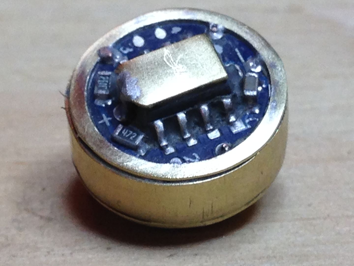
I like the strap idea since it takes battery pressure off the mcu but with just a wire over the top as B+ a dab of epoxy under the mcu before soldering should help support the mcu. The pill pictured above is solid JB weld between the pins and underneath the mcu and took some delicate work with a q-tip and solvent to clear the pins. I’m hoping it can still be reflashed set up this way but don’t have a clue really. That pill is for the smaller of the ladies night clickies(2-mode, 20/80% single 350mA 7135). The light functions perfectly but I had a major failure in the metal work and had to order some different brass.
While I haven’t actually built any 10mm drivers, I really don’t see a problem with the MCU taking the brunt of the physical battery-compression forces. I think that the legs should crush/bend slightly and then the MCU will be flat against the PCB: no harm, no foul.
That looks nice! I’ve got a couple of boards on the way from OSH Park where I’ve had this in mind, purely motivated out of being tired of ripping my lights apart to flash them with new firmware. I’m thinking a slightly bent copper plate to act a little as a spring for the cell, thin enough to allow me to flash it without removing it. Your solution looks good.
Am I seeing correctly? The middle of the 3 legs on the 7135 chip that’s ground doesn’t have ground under it, but there is a pad there… is this correct? That pin can be removed and with the middle of the board fairly clear a small post or pillar can be glued to the pcb. This can be the battery contact point, on the fet side of the board, with a connecting wire from the + via.
The MCU is too thick to be on the battery contact side of my TP.