Nanjg AK-47A Chip ID

I’m slowly making progress on understanding these little circuits and how to reprogram them (STAR, minidrv, etc.)

I was mucking around with one last night and realized I don’t know what the component near the positive out is.

Anybody know what chip this is?

What it does?

Please ignore the other red box I was showing someone else where to solder a capacitor for off time memory.

Can’t seem to get a picture to post inline so here’s a direct link.

http://s256.photobucket.com/user/headie_fishing/media/Driver%20Circuit.png.html?o=0

Thanks!

That’s a diode. The attiny13 will be fried if it gets reverse polarity so the diode protects it in case you insert a battery backwards.

Halo - big help. I always wondered how the reverse polarity protection was implemented.

Any ideas as to what type/size/etc diode it is?

Yep! Schottky diode. See this thread on selecting an appropriate one. https://budgetlightforum.com/t/-/34123
As for size, iirc its SOD-323. But any size that fits can work.

Thanks - I’ll see if I can absorb some of it.

Any idea if there’s a schematic for the AK-47A floating around anywhere?

Something like post #14 here (105c): LED Driver Schematic

Or the multi-colored photo at the bottom here (also 105c): AVR Drivers - Flashlight Wiki

The AK-47A and most of the other chinese attiny13 amc7135 boards share the same schematic as the nanjg 105c from post #14

Or are you more looking for an actual pic of the AK-47A with the different traces identified like the 105c pic on flashlightwiki.com?

There is this pic.

Thanks for sharing the schematic. I came across that in my search but I’m a bit unlearned as of yet and was hoping for something that mapped it’s way through all of the components (even the duplicates like the 7135s) and especially the AK-47A vs the 105C.

Something more akin to the color photo from the tutorial would be most helpful.

Edit: I also came across the second photo you posted. I guess I was hoping for some combination of the two but I suppose I’ll need to roll up my sleeves a bit and fill in some blanks.

I’m also using an extra capacitor in R4 for STAR Off time memory and wonder how that’s wired in.

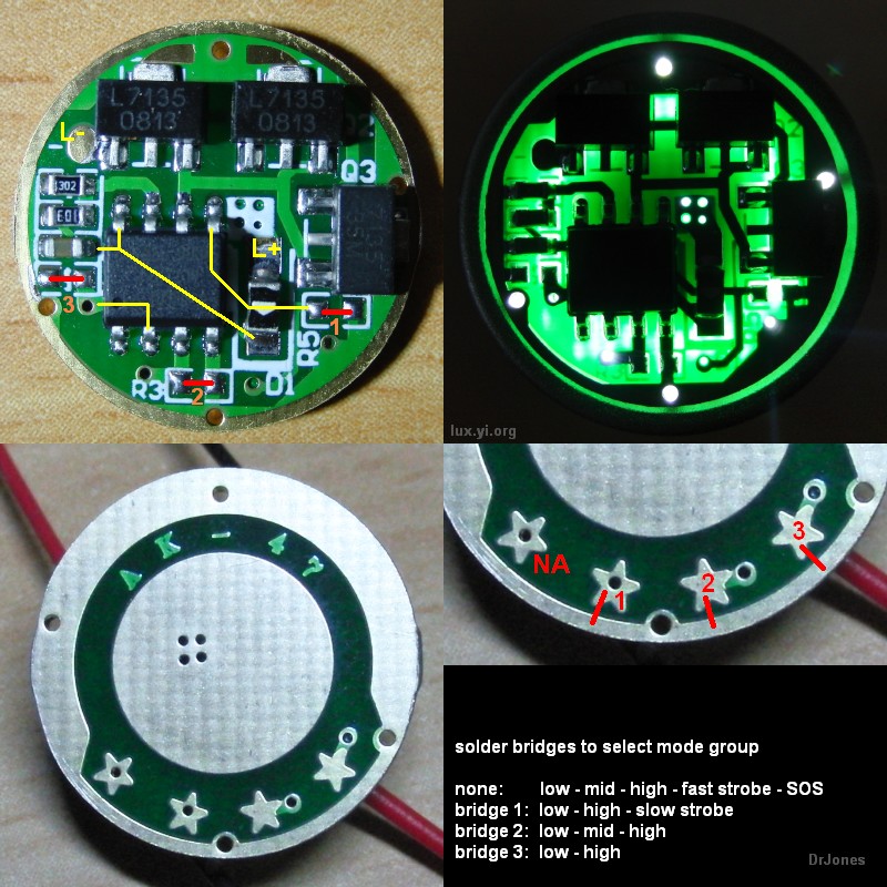
Is the schematic understandable, as far as showing how parts connect to the attiny? I mean, I know it uses component symbols instead of actually labeling everything. Are you familiar with all the symbols there (diode, capacitor, resistor and ground)?

The off time capacitor is connected between ground and pin 2.

With the ak47 the attiny is oriented with the “reset” pin (pin 1) bottom left. So looking at the DrJones ak47 pic, you can follow the yellow line from R4 (labeled “3” in the pic) to pin 2 on the attiny. Schematic shows pin 2 is aka PB3 (when talking about firmware code).

THIS is useful info. THNX

Halo - this was all very helpful and it just occurred to me that I had not responded!

Thanks a bunch for your help.