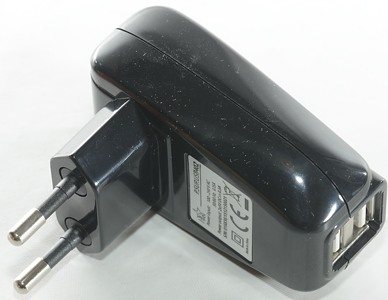
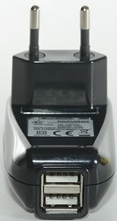
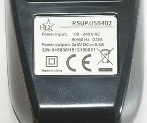
HQ Universal USB charger dual output P.SUB.USB402
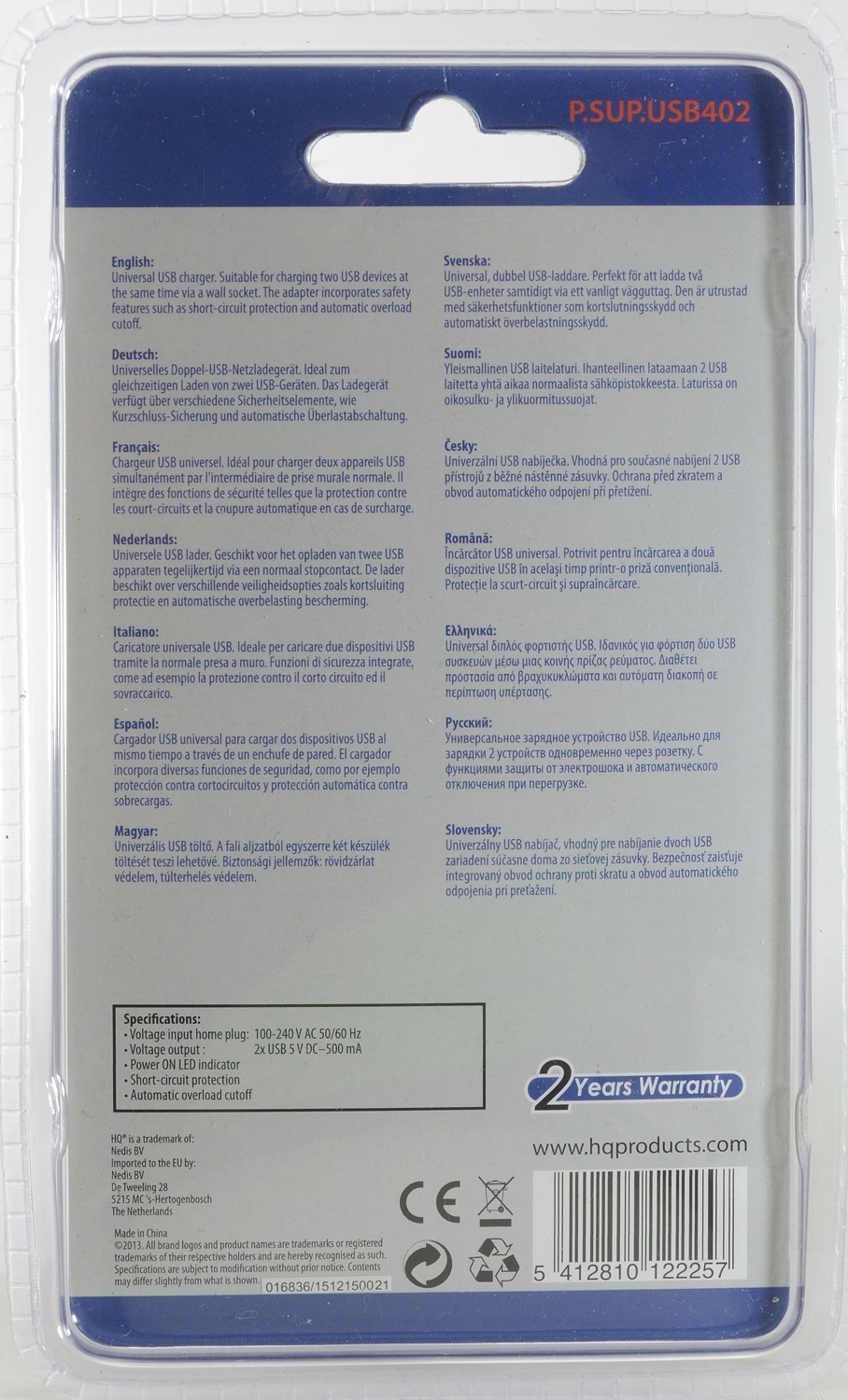
Official specifications:
-
Outputs: 2
-
Cable: No Cable Included
-
Color: Sort
-
Connector type: USB
-
Output voltage:5 VDC
-
Connector type: Euro / Type C (CEE 7/16)
-
Input voltage: 100-240 VAC
-
Max output current for each port: 0.5 A
-
Total output current: 1.0 A

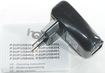
The box contains the charger and a multi language and multi device instruction/data sheet without any useful information.
Measurements
-
Power consumption when idle is 0.2 watt
-
Both usb outputs are coded as Apple 2.4A
-
Usb outputs are in parallel.
-
Weight: 50.5g
-
Size: 65 x 62 x41mm
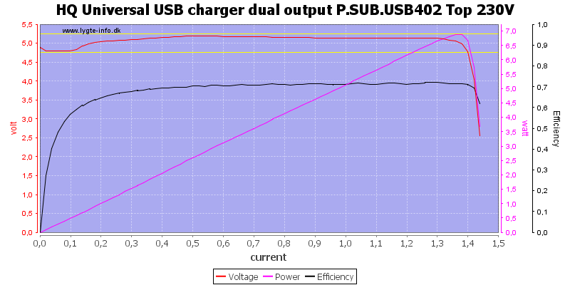
One output can deliver 1.4A, before it shuts down.
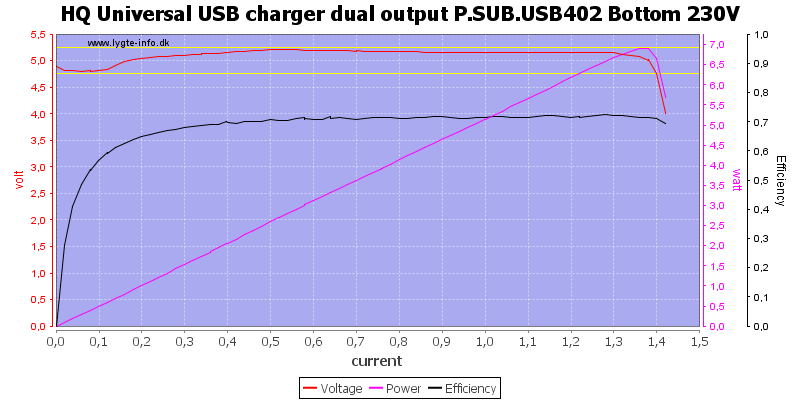
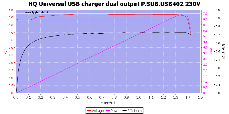
Both outputs together is also 1.4A.
At low load the output voltage drops a bit, then it is increased.
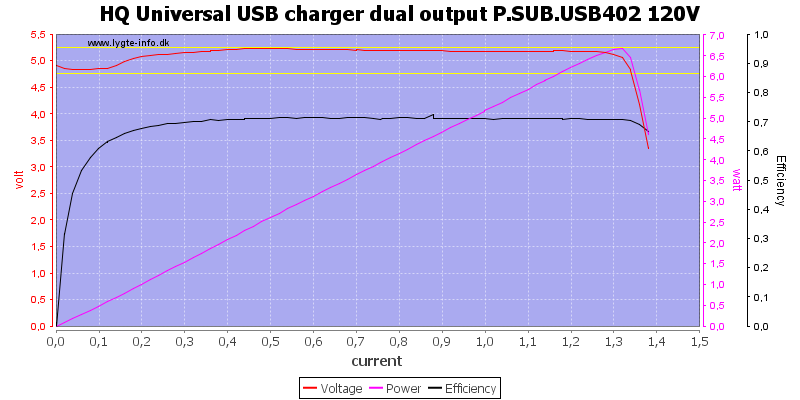
At 120VAC the output current is reduced slightly to 1.3A.
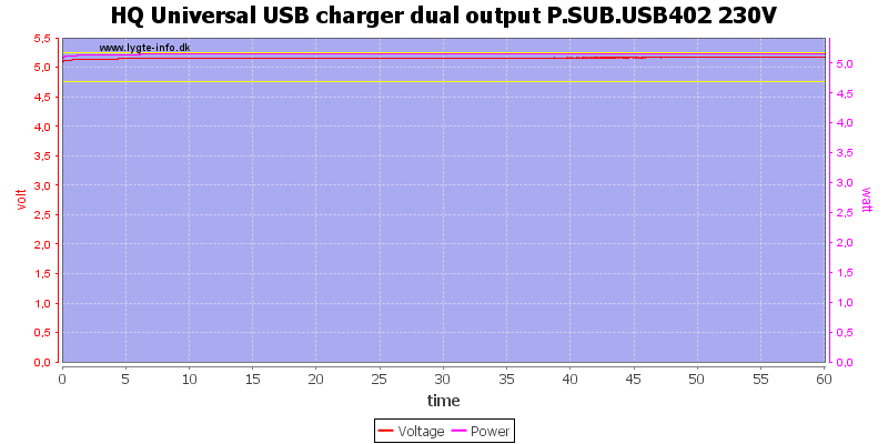
There is no problem delivering the rated 1A current for 1 hour.
The temperature photos below are taken between 30 minutes and 60 minutes into the one hour test.
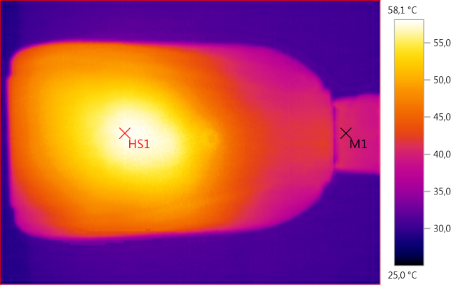
M1: 40,6°C, HS1: 58,1°C
HS1 is the transformer.
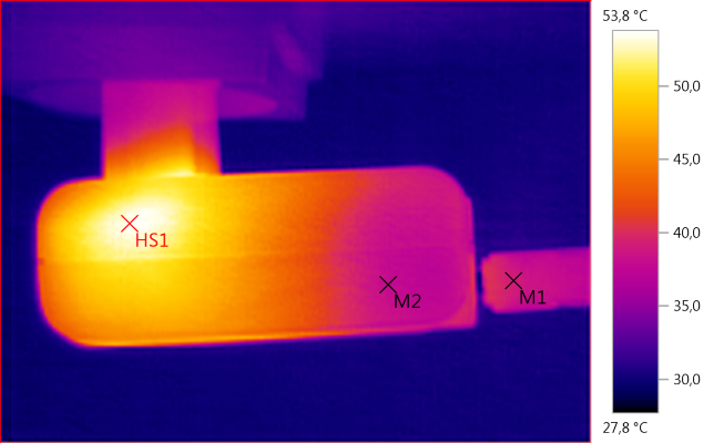
M1: 39,2°C, M2: 37,9°C, HS1: 53,8°C
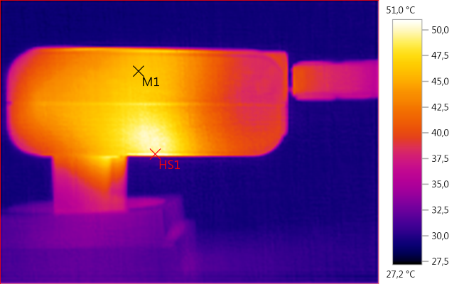
M1: 46,1°C, HS1: 51,0°C
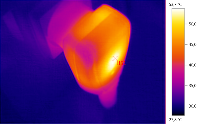
HS153,7°C
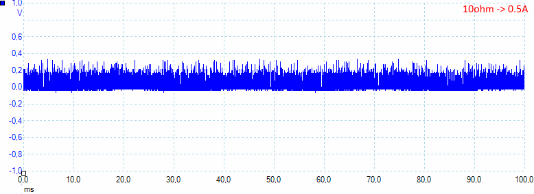
At 0.5A the noise is 74mV rms and 428mVpp.
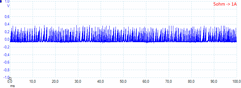
At 1A the noise is 98mV rms and 459mVpp.
Tear down
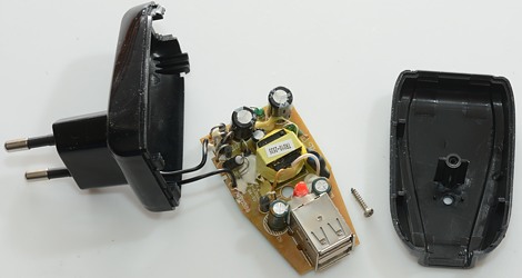
Removing one screw and a bit of force was required to open this charger (There are some clips in addition to the screw).
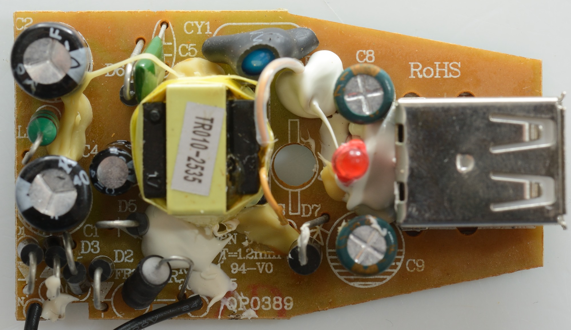
The circuit board looks a bit messy with all the leaded components and the white glue.
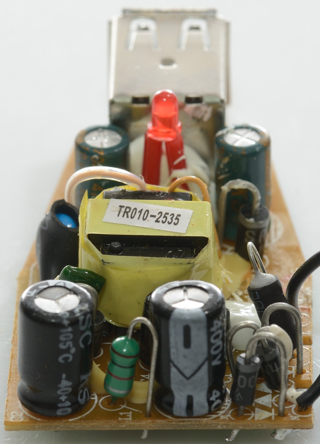
At the input there is a fuse (Fusible resistor) and a bridge rectifier made with four diodes (D1-D4). Between the two capacitors (C1, C2) is a inductor (L1). The safety capacitor (CY1) is covered in heatshrink.
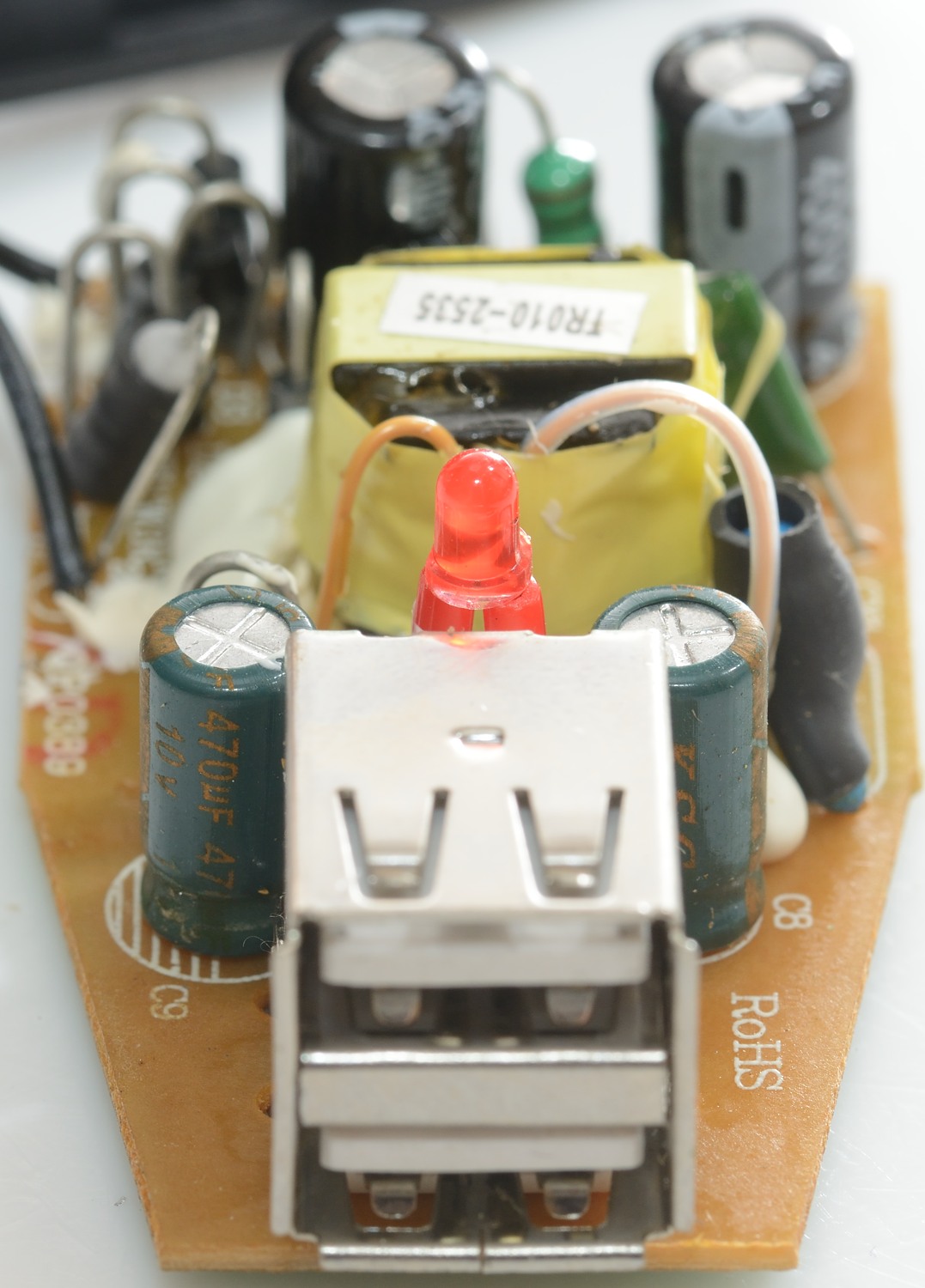
The transformer uses flying leads for low voltage output, this will improve the isolation distance. On the low volt side there is a rectifying diode (D7) and the red indicator led.
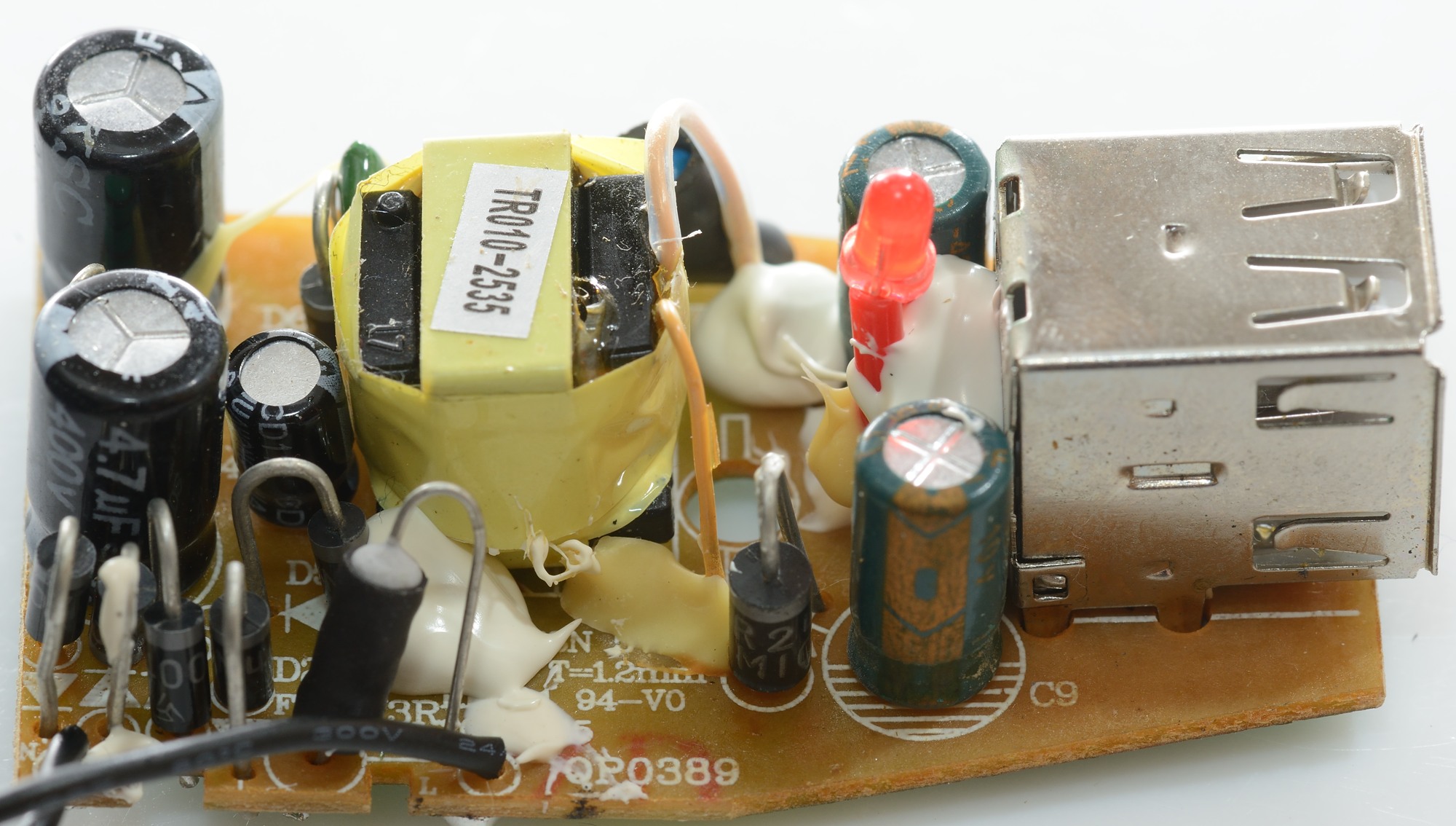
On the second picture the inductor (L1) is easy too see, the bridge rectifier is made with four 1N4007 diodes, this is a very old and very common type diode.
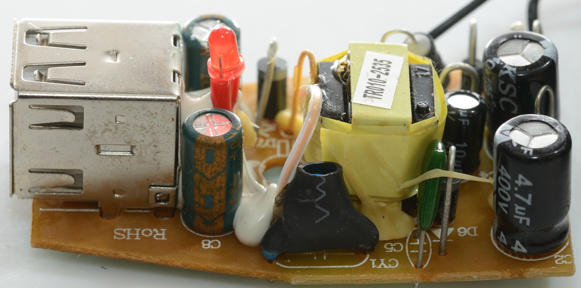
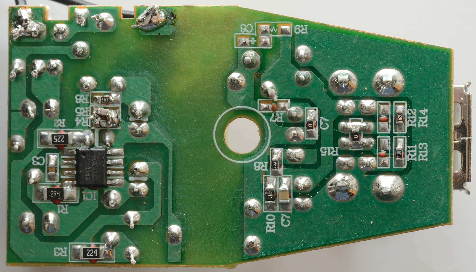
The mains switcher IC is a AX2535, the soldering/mounting looks rather bad for R5.
The usb coding is made a very simple way with two resistors.
Creepage distance is well above 6mm.
Testing with 2830 volt and 4242 volt between mains and low volt side, did not show any safety problems.
Conclusion
The charger can deliver the rated current, but the current is low for single usb output and more so with a dual usb output, the charger looks safe. The coding of the usb output is wrong and the noise is slightly high.
The charger is fine for most low power applications, but not for smartphone charging or high power applications.
Notes
Charger was supplied by Pro backup (probackup.nl)
Read more about how I test USB power supplies/charger
How does a usb charger work?