Hello friends. I’m working on an unconventional build. I’ve chosen to use the driver from the sunwayman t25c because it is suposed to work with input voltage up to 8.4 and is also a clicky switch UI.
While testing I found the driver to get very hot when above 6v and on high mode. The wattage between 6v –8v is between 12-13 watts. I found the heat to be coming from the ss54 marked diode. I have looked at the data sheet for this diode and according to the specs it should be fine running at 8v 1-2amps. Or maybe it is on the led side of the driver? In that case the operating parameters would be 3.5v and 3-4amps. But this is still within specs.
When I say hot, I mean within 20-30sec it unsoldered a lead that was on the grounding ring next to the diode.
Can someone share some knowledge that may help me here? Would replacing the diode help in this case?
If I have to, there is an r015 resistor that I could change to lower the output some. I don’t need it to be at 12-13 watts for this application. However the diode gets got pretty quick on the next lowest mode as well. That is only 7.5watts. So…
As I see in your picture , there is something wrong with the FET transistor , limit resistor (R015) and the red wire (+ Led) !
By no mean the gate can NOT be connected thru the R015 to the Source and to red wire (+ Led). The small transistor has the 3 pins like : 1=gate , 2=drain , 3=source.
When you soldered the red wire for the + led , you connected also the gate of the transistor ,so , the CORRECT connection is : pin 3 transistor to R015 and the other side of R015 direct to red wire ! Redo the solder to the red wire in such a way to NOT touch the pin1 of the transistor !
The diode is good as it is but , because of what you've done, I'm suggesting to check the diode , the transistor and R015 (in the picture seems to be over heated )
That’s interesting, but I have not soldered anything on this driver. The driver in the picture has been untouched. The driver that I’ve been working with is exactly the same. Are you sure there is a problem here? The light works as it should with 4.2v but gets extremely hot when in high and 8.4v.
As per the layout I see , the transistor is a P-channel MosFet . It means that with R015 connected source-gate it will be ALL the time in ON state , regardless PWM coming from MCU. Is becoming a DD ( Direct Drive) , where ALL the current the batteries are capable of , is gone get to load . So , bigger voltage - bigger power dissipation , less voltage , less power ! In a regulated driver , double voltage means half current in the driver ( in theory , at least).
With 4.2 V in direct drive a led can survive due to resistance of springs , wires , connections, but on 8.4 V , I doubt ...
I'm telling you again that that solder is wrong , and if you don't believe it , let's wait for some others guys to step in.., I'm sure that , at least a dozen of them will figure what I'm talking about...
It’s not that I don’t believe you in that it’s not right. But the led is not seeing direct drive. It is regulated through all the modes as it should it’s just that the driver is over heating. If it were direct drive at 8.4v my led would not have lasted 30s. I’m powering this from a power supply do I’m able to watch what is happening power wise. All the way from 4v to 8v the driver is consistently regulating the power between 11.5-12.5 watts. When I raise the volts, it uses less amps. So it’s figuring out how to measure current somewhere on the driver.
also, I have a whole box of these lights. The three that I have opened up are all the same so if the component placement is incorrect it’s not a random mistake. Hmm? If the resistor is misplaced is it still possible for the driver to regulate?
Have to head out soon but I thought I'd drop a quick reply. To understand the problem, let's first try to figure out the circuit.
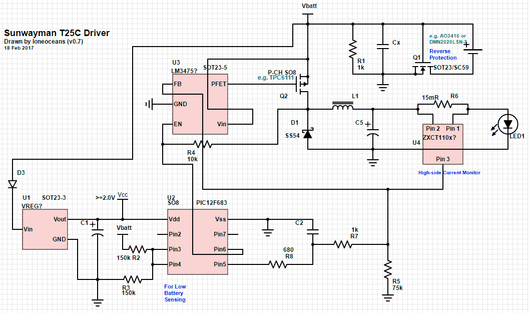
The driver in question definitely looks like some sort of regulated driver, specifically a Buck Controller. The photo you have is a little unclear and I can't see what the bottom is (photo would be useful!) but U3 is the main buck controller, D1 is the catch diode, L1 is the main buck inductor, Q2 is the main P-Fet in a SOT23-5 package, and U2 is likely the small MCU in charge of the smarts.
What is a little unclear to be is to purpose of U4. Somehow since there are different modes and I suspect this driver is constant current regulated (please verify for me that the light does not flicker / no PWM at lower brightness settings - if it does we'll have another point to work off from), there needs to be some sort of feedback control. So R6 could be some sort of either current sense or current limiting resistor. It's a little hard to see from the photo so let me think about it a bit more. As you can see, the top of U4 feeds to pin 1 of U3 which I'm pretty sure is the FB pin. This is connected via some resistors to pin 5 of the MCU, so output can be regulated in some way.
It's strange that the diode is getting so hot since it looks like a decent diode. Let's assume you have 8.4V 12W in 3V output, the average current across the diode is 2-3A with higher peak. Let's assume it's 3A with a 0.5V V_fwd, the diode is dissipating some 1.5W in conduction losses and more due to reverse recovery. On the other hand, at lower input voltages, say 4V, the diode average current drops to 0.75A. So out of the bunch, the diode is likely the one that's dissipating the most power, more so than the FET (depending on the fet) or the inductor.
Unfortunately this doesn't answer your question (yet), but let's see if we can figure it out :)
Loneoceans, thanks for taking the time to give some input!
I was surprised to see that the light does have some PWM. Subtle lines can be seen when taking video.
I will take your circuit information and try to understand the layout a bit more tomorrow. Anyone else feel free the give your thoughts.
Edit: If the diode has to dissipate 1.5 watts, that means the diode will be 90C above ambient. This is pretty hot, but shouldn’t be hot enough to melt solder. To melt solder, the diode would have to be dissipating almost 3watts. So, something isn’t right. Does the switching frequency affect the diode at all?
Didn't follow all the replies. Yes the diode is probably on the low side, but it only sees current when the buck FET is off (when it's shedding voltage).
The diode power loss in watts is approximately Vf * (1-Vo/Vi)*Io
Vf: diode forward voltage
Io: Output current to LED
Vo: Output voltage to LEd
Vi: Input voltage.
1-Vo/Vi is the duty cycle for the diode. As you go to higher input voltage it gets higher. At very low input voltage, it gets near zero.
So just work out what this is in watts and look up the thermal resistance of the component in C/W and you'll get a rough feel for the temps to expect.
Anyway, the diode is definitely one of the biggest bottle necks for heat and losses in a buck that's being used to drop volts. Also if it gets too hot it can stop acting like a diode and start acting like a 2-way resistor further decreasing efficiency and increasing heat.
Using your equation I get 1watt at her diode so in theory it shouldn’t be getting so hot.
Idk if this is helpfull at all? I’ll look at the circuit more closely tomorrow. I was surprised to find that there is only one point of connection to B- in this circuit.
That doesn't mean 1W flowing through it. It means 1W of heat dissipation/power-loss. That's not small. I'll see if I can see what the data sheet says about it. I wouldn't be surprised to like 80C/W.
I spent about 10mins doing a quick exercise trying to figure out the schematic from the photo above... I'm fairly confident of most of the items but there are some aspects which I'm not sure. Specifically if you could post a photo of the bottom of the driver and help me verify the following, that would be useful!
I expect one of the pins of U2 to be connected to R2.. could you verify which pin it is?
Likewise, is R4 connected to any of the pins of U2?
What are Pins 2, 7 and 8 connected to (of U2?)
Could you check if D3 is indeed wired correctly as shown?
I know this doesn't really help solve your problem, but it's a useful exercise and hopefully will be useful for other people in the future. Once I figure it out I can update the schematic. Right now I'm unsure as to what U4 is. Any suggestions would be welcomed.
Now answering your questions, we can estimate the loss of the catch diode = V_fwd x I_avg
I_avg = (1 - Vout/Vin ) * I_out
Let's assume Vout = 3V, Vin = 8.2V, total P = 13W, V_fwd = 0.5V and I_out = 4.33A, then P_fwd_loss = 1.37W
Next the diode reverse recovery loss = Q_rr * Vin * f_sw
I have no idea what the switching frequency is nor Q_rr, but I suppose we can assume the total diode loss is around ~2W.
So even with no heatsinking, your diode should not be performing so poorly (i.e. maximum temperature rise would be 30degC for 15C/W).. however I feel like that's a bit suspect because comparing other similar SMC packages, the junction to lead being ~15C/W sounds reasonable, and ~100C/W junction to ambient being more reasonable. That said, the diode also is connected to the ground plane which should act as a heatsink... it'll probably get warm but the numbers don't seem concerning yet.
In any case, I suppose I find it a little unusual that the part would get so hot as to solder itself off considering that everything looks to be designed fairly ok..
It's pretty late now so I'll look at it a little more tomorrow :)
The shcottky has the full output current running through it, but at 50% duty cycle. loneoceans diagram looks about right. It's not a protection diode it's a freewheel diode. But I agree with light rider that 1W in that diode should not be melting things.
loneocean U4 is an amplifier. Nice daigram. That's actually kind of cool. That buck controller is designed to be voltage controlling but by adding a sense resistor and and amp they've made it current regulating (not a terribly uncommon trick). The neat thing is it kind of looks like they might be doing something similar to what we did with the texas buck, which is sending pwm from an mcu through a low pass filter to adjust the regulation. I'm not quite certain though, as I don't quite understand that how pin3 of u4 interacts with all that, but that does seem to be the point. This is likely to be a true current adjusting non-PWM buck.
What I don't get (and it may just be that I don't get it) is why put the sense on the output current instead of the inductor current. It seems to me you could essentially eliminate output ripple just by putting the sense resistor on the inductor current, because the output fluctuations are much smaller than the inductor fluctuations if the caps are chosen right, but the average current is the same.
I’ll be headed to the bench in a bit. Are there any data points or measurements that I can provide while testing? I will compare the circuit above to the board as well.
Ok here is a sketch of all the connections on the driver. It’s a mess and let me know if it can’t be understood and I can redraw it. The pic is 12F683 and the datasheet is easily found on google search