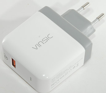
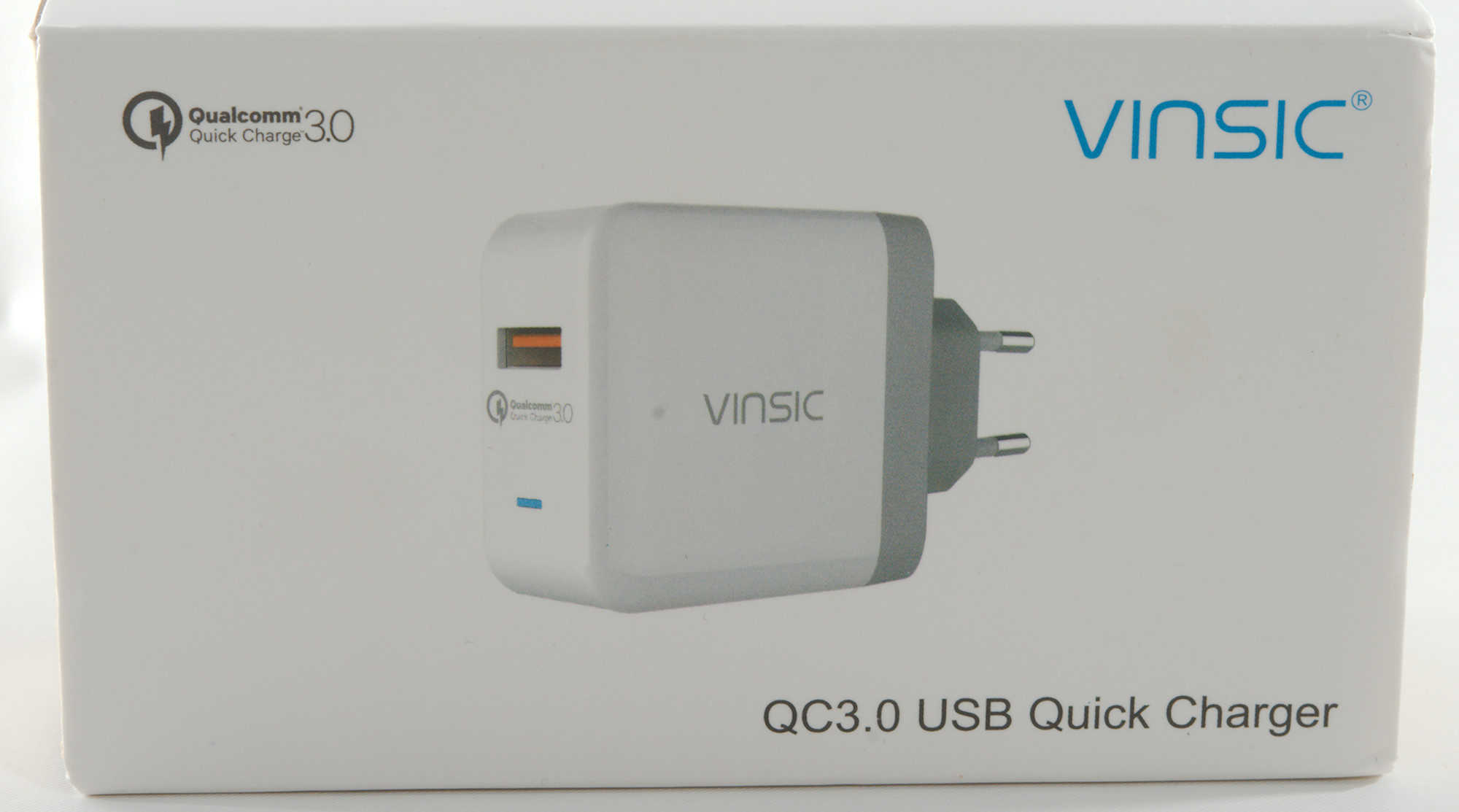
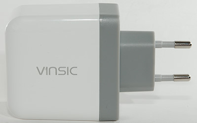
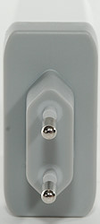
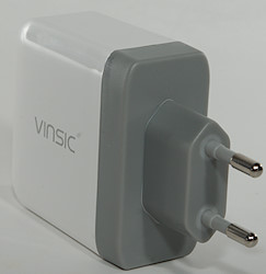
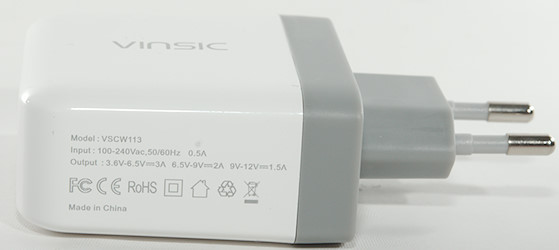
Vinsic QC3 charger VSCW113
Official specifications:
-
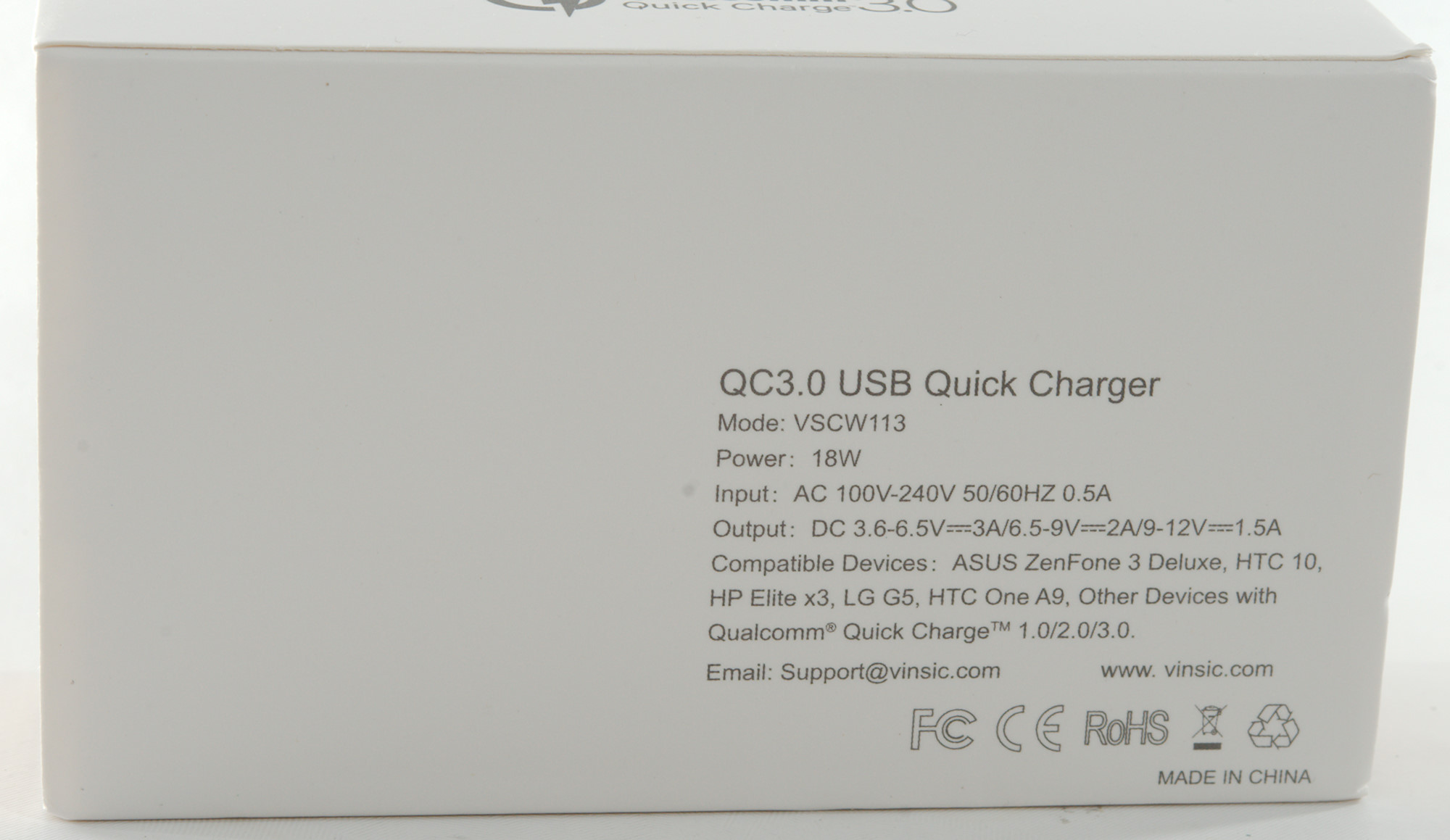
Input: AC 100-240V 50/60HZ 0.5A Max
-
Output: 3.6V-6.5V 3A, 6.5V-9V 2A, 9V-12V 1.5A
-
Power: 18W
-
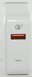
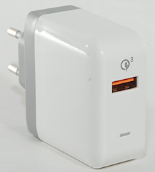
Qualcomm Quick Charge: 1.0, 2.0, 3.0
I got it from a Aliexpress dealer: VINSIC Official Store
It was in a white box with specifications on the back.
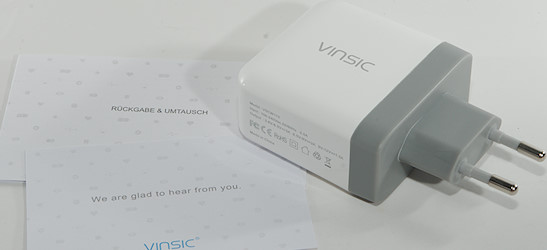
The contents was only the charger.
Measurements
-
Usb output is coded as QC
-
Power consumption when idle is 0.08 watt
-
Minimum QC3 voltage is 4 volt, going one step lower will reset the output.
-
Indicator light is blue when output is 5V and green when output is 9V or 12V
-
Weight: 75.2g
-
Size: 94 x 57 x 28mm
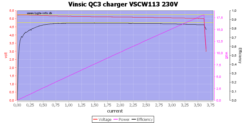
It is rated for 3A at 5V and can deliver 3.6A, this is fine.
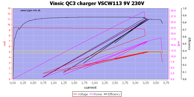
At 9V it is only rated for 2A, but can deliver above 3A, before drops to 5V. It turns the power off shortly before dropping to 5V.
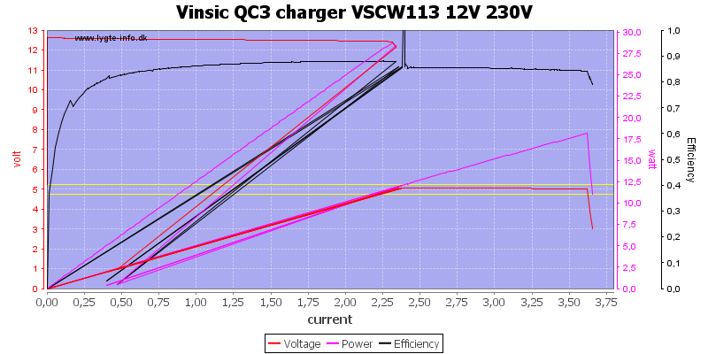
At 12V t can deliver 2.3A before dropping to 5V. It turns the power off shortly before dropping to 5V.
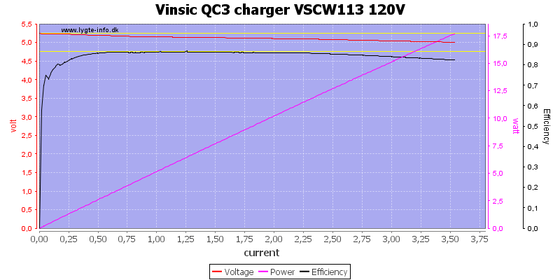
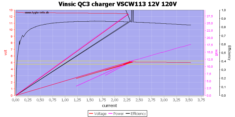
It works the same way with 120V mains voltage, but the current is slightly lower.
No problems running one hour at 12V 1.5A.
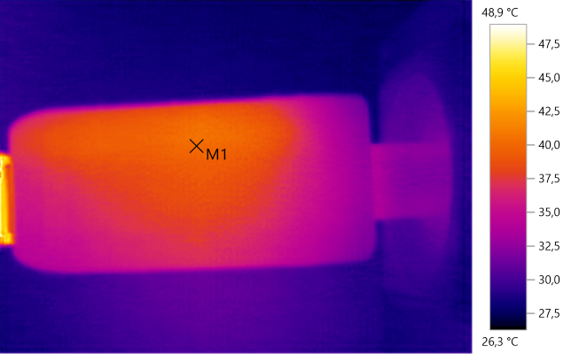
The temperature photos below are taken between 30 minutes and 60 minutes into the one hour test.
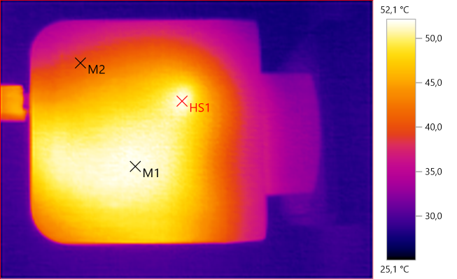
M1: 51,7°C, M2: 40,1°C, HS1: 52,1°C
M1 is the transformer and HS1 matches a capacitor, but I would not expect that to show a heat signature. The reason is probably because the white stuff touches the plastic here and it is transferring heat much better than air.
M1: 40,2°C
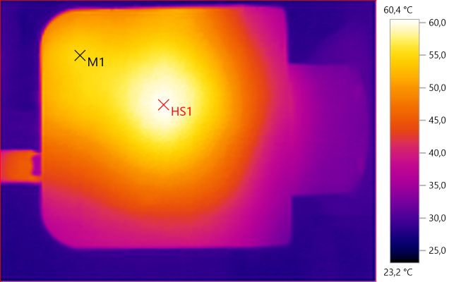
M1: 54,9°C, HS1: 60,4°C
HS1 is again the transformer.
M1 is the rectifier.
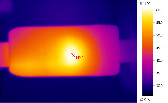
HS1: 61,1°C
HS1 is the transformer and matches the white stuff that is between the transformer and the plastic.
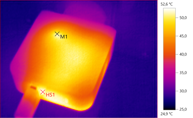
M1: 50,8°C, HS1: 52,6°C
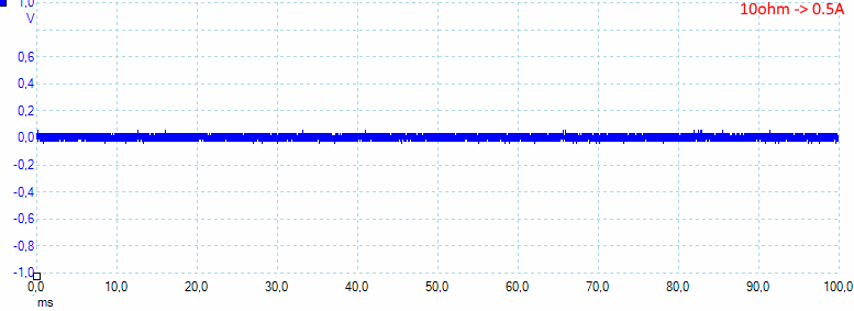
At 0.5A the noise is 20mV rms and 124mVpp
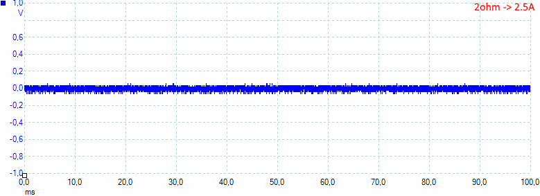
At 1A the noise is 34mV rms and 166mVpp
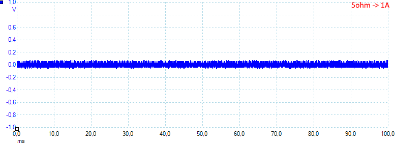
At 2.5A the noise is 32mV rms and 156mVpp
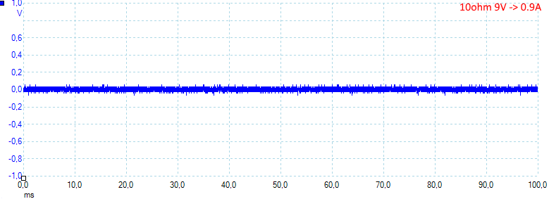
At 0.9A the noise is 25mV rms and 149mVpp
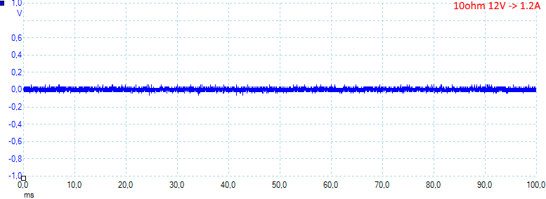
At 1.2A the noise is 27mV rms and 156mVpp, all results are low.
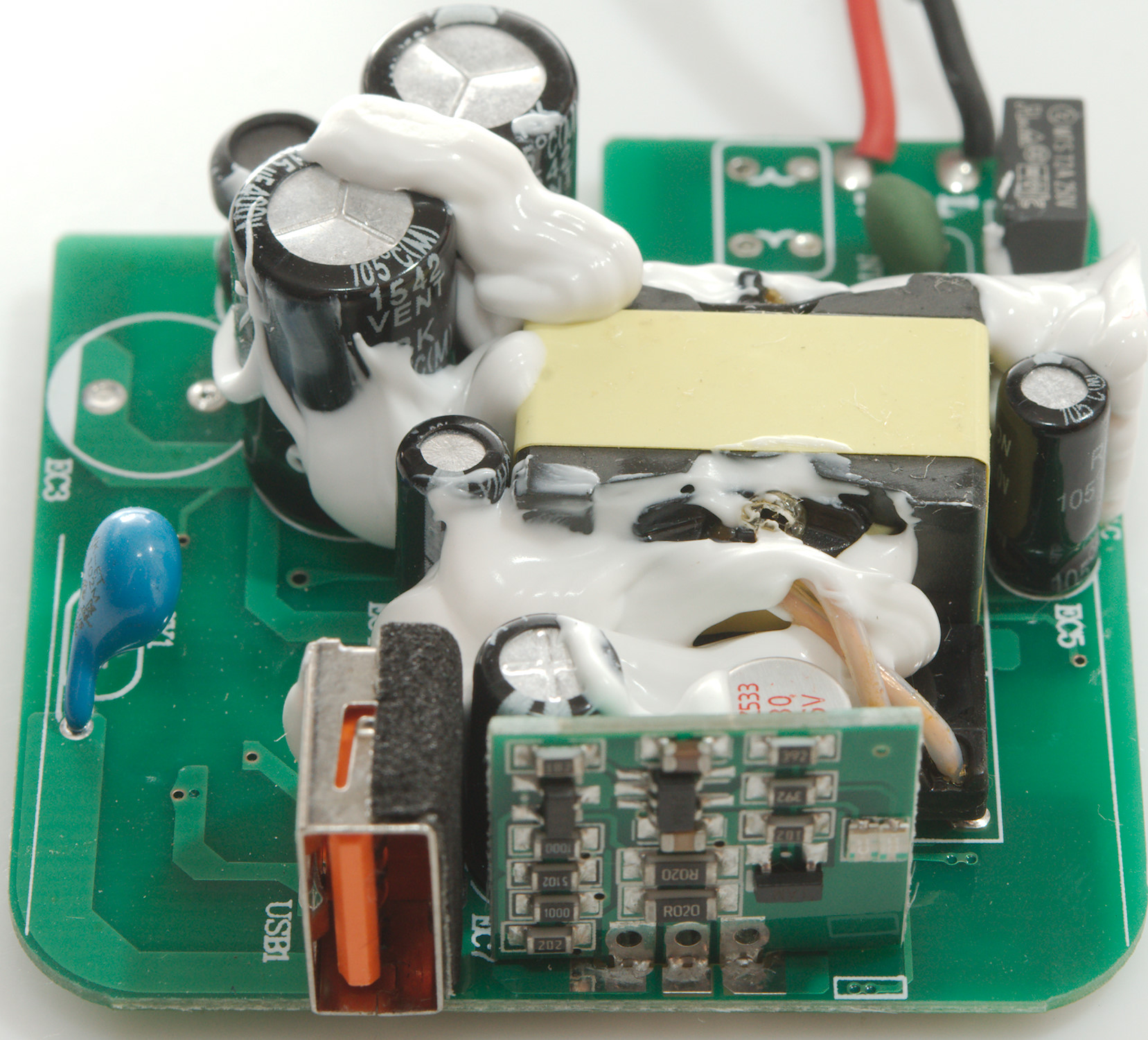
Tear down
Mounting it in my vice and whacking it a few times with my mallet and it was open.

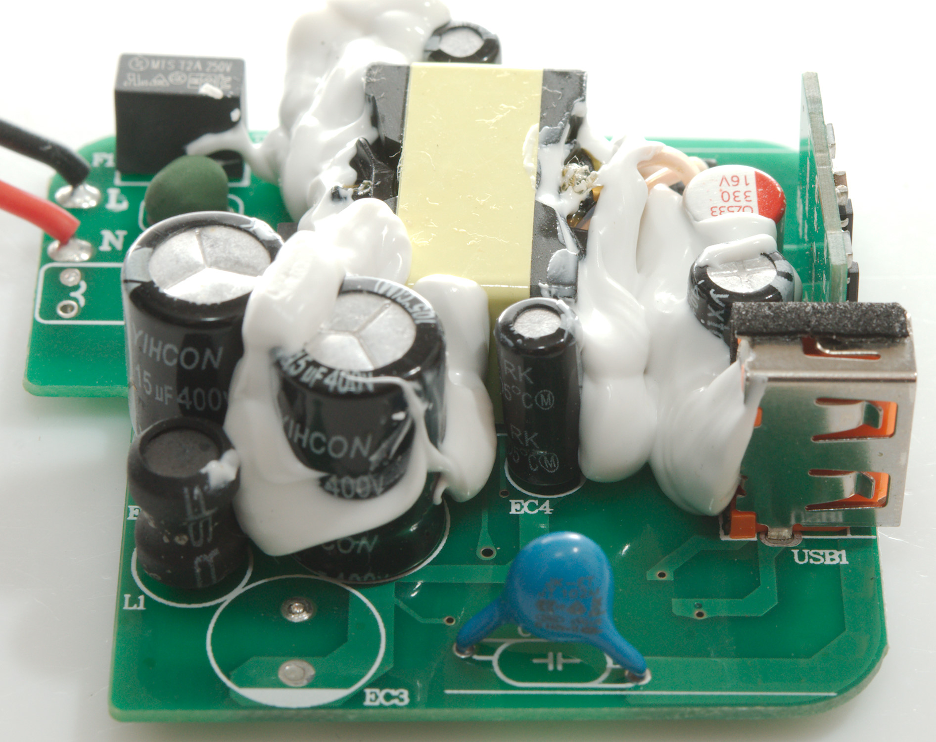
At the mains input is a fuse and a inrush current limiter (NTC1), the common mode coil is missing (LF1). There is an inductor (L1) between the two mains capacitors (Space for 3). The mains switcher transistor (Q1) is placed against the transformer.
There is a blue safety capacitor.
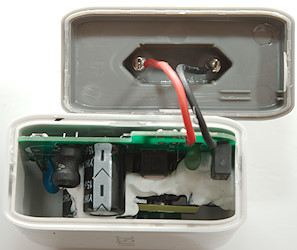
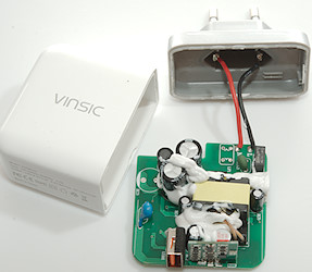
At the output is two capacitors and a small circuit board. The transformer has an extension for the low volt connections.
The first picture shows the safety capacitors, on the second picture is the small circuit board.


On the second picture the mains switcher transistor (Q1) can be seen.
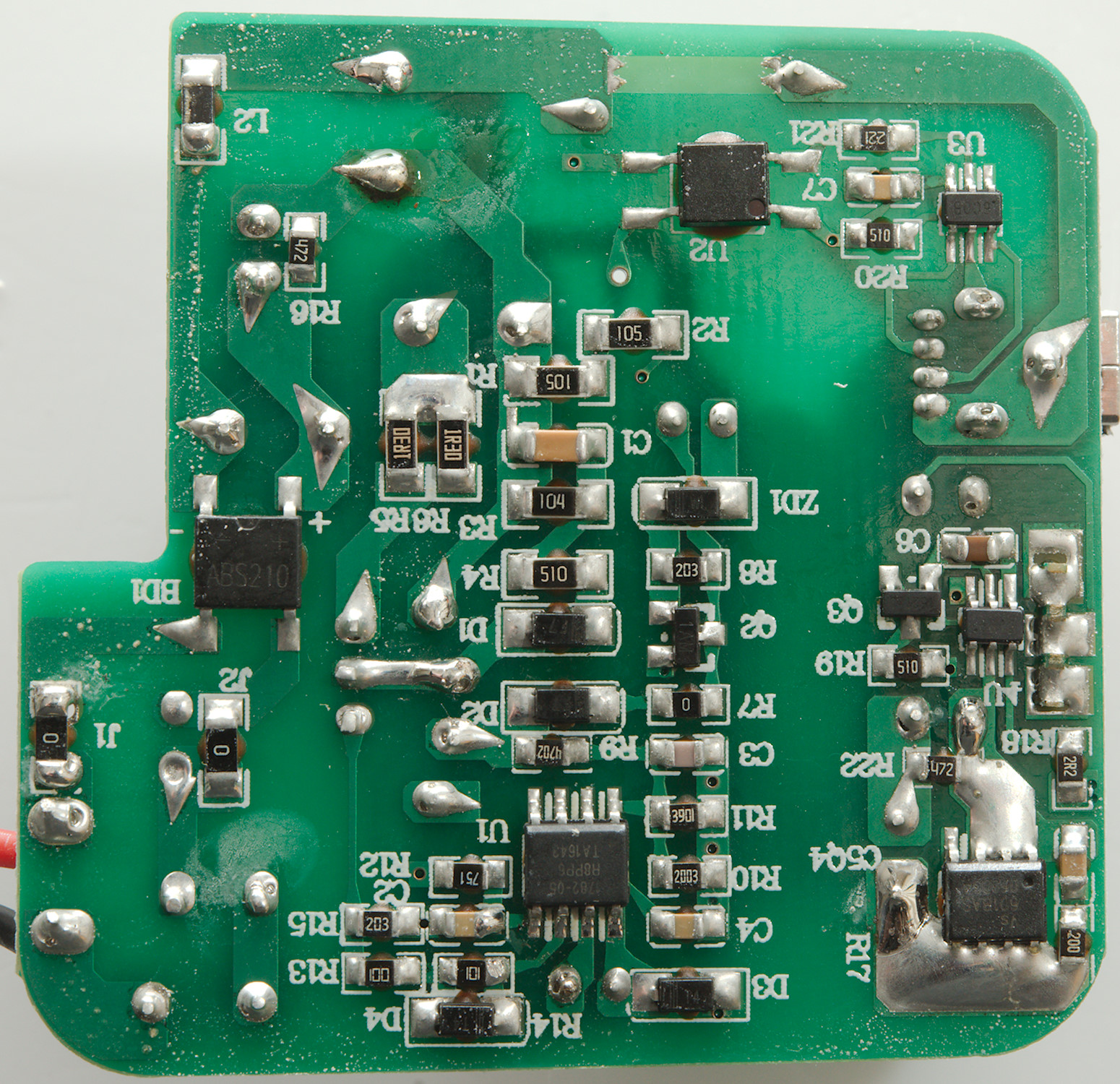
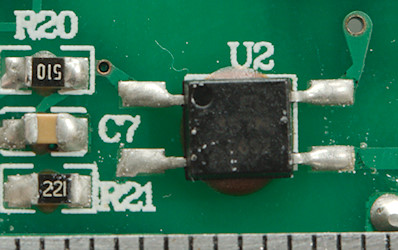
At the mains input is a bridge rectifier (BD1). The mains switcher controller (U1), it looks like the power supply for this controller is stabilized with ZD1 and Q2. The optocoupler is U2 and it is controlled from the QC controller (U3).
The rectification is synchronous with a transistor (Q4) and a IC (U4).

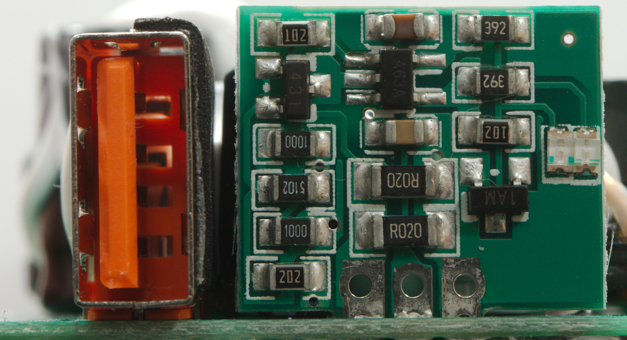
The small circuit board is for controlling the blue/green leds. There is a reference (431), probably an OpAmp and a transistor.
It also looks like the full output current is routed through this board (2xR020 resistors), but I do not believe it is used for anything.
Safety distance look good.
Testing with 2830 volt and 4242 volt between mains and low volt side, did not show any safety problems.
Conclusion
This charger is a fairly good QC2 charger, but I do not like that it resets its output voltage when QC3 selects a low voltage.
Noise, safety and output power all looks good.
Notes
Index of all tested USB power supplies/chargers
Read more about how I test USB power supplies/charger
How does a usb charger work?