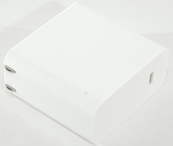
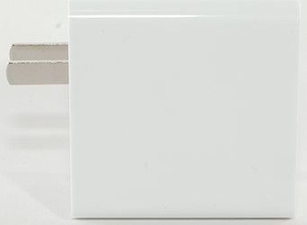
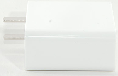
Xiaomi Mi 45W USB-C charger CDQ02ZM
Official specifications:
-
45W Max Smart Output
-
5V=3A/9V=3A/12V=3A/15V=3A/20V=2.25A
-
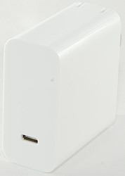
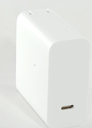
Type-C Port
-
USB PD 2.0 Quick Charge QC 3.0
-
Free Gift: Cable Type-C to Type-C
-
Xiaomi USB-C Power Adapter (45W)
I got is from Aliexpress dealer: MI-homes Store
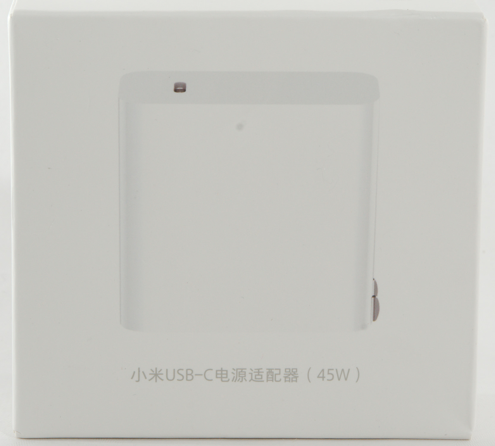

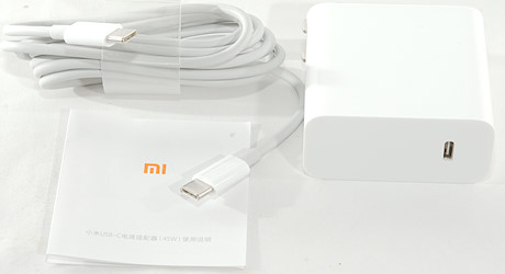
The box contained the charger, instruction sheet in Chinese and usb-C cable.
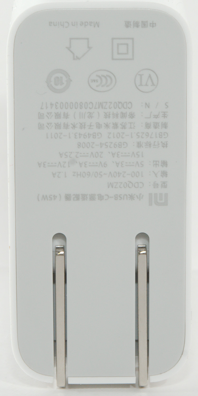
Measurements
-
Power consumption when idle is 0.05 watt at 230VAC
-
PD modes: 5V 3A, 9V 3A, 12V 3A, 15V 3A, 20V 2.25A
-
PD port also supports: DCP and QC3 up to 12V
-
Minimum QC3 voltage is 3.7V
-
Default state for output is off.
-
Size: 62 x 57 x 28mm
-
Weight: 102g
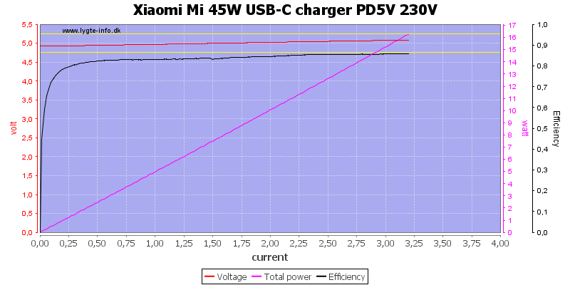
At 5V then charger can deliver 3.2A, this is fine for a 3A rating. The charger has some cable compensation and the output voltage raises with higher load current.
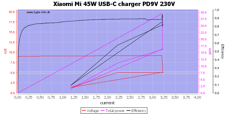
At 9V the overload protection also trips at 3.2A
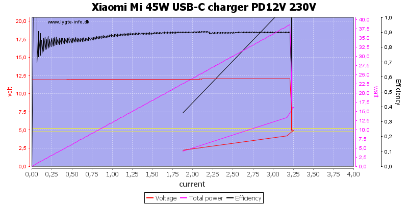
At 12V it is again 3.2A
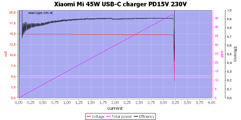
And at 15V the same. It looks the the cable compensation is disabled at this voltage, this is fine enough, there is no reason for it at this voltage.
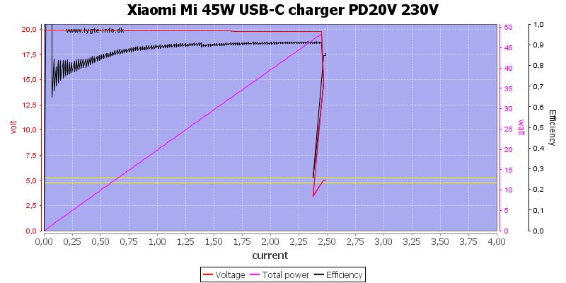
At 20V the maximum current is reduced to 2.5A
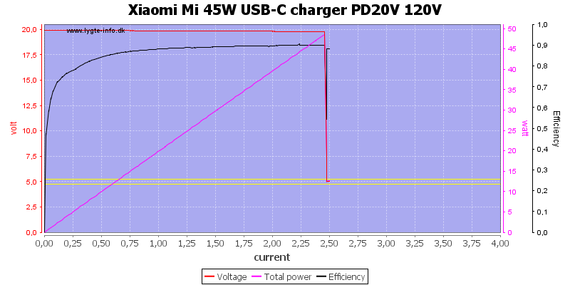
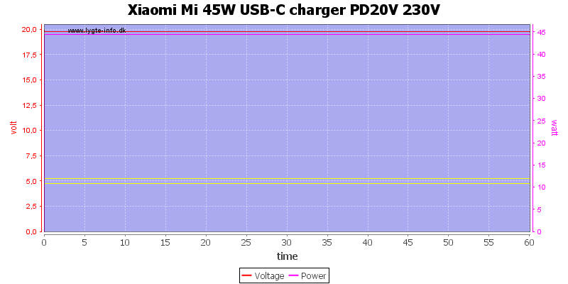
This is exactly the same at 120VAC.
Running at 20V 2.25A for one hour did not show any problems.
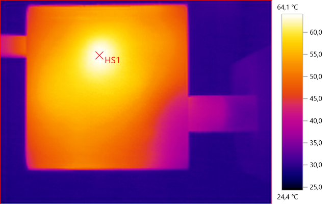
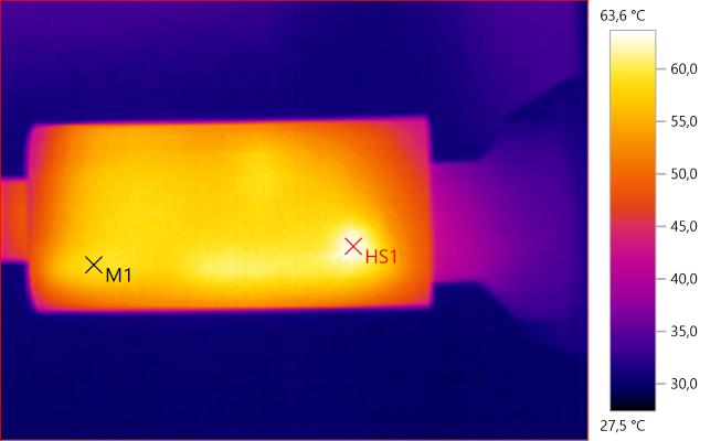
The temperature photos below are taken between 30 minutes and 60 minutes into the one hour test.
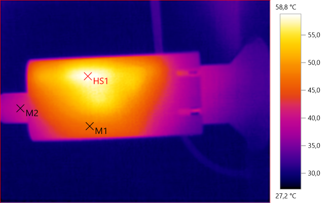
M1: 47.2°C, M2: 40.1°C, HS1: 58.8°C
HS1 is the heatsink for the main switcher transistor and transformer.
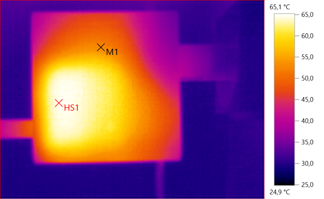
M1: 52.9°C, HS1: 65.1°C
HS1: 64.1°C
M1: 58.9°C, HS1: 63.6°C
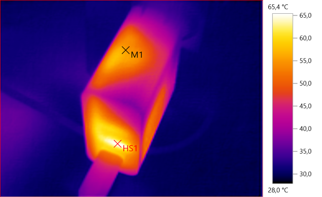
M1: 55.6°C, HS1: 65.4°C
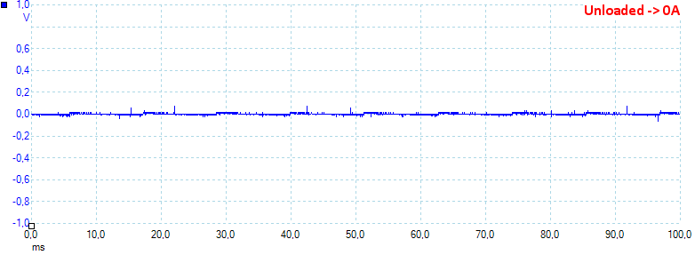
Unloaded the noise is 7mV rms and 136mVpp
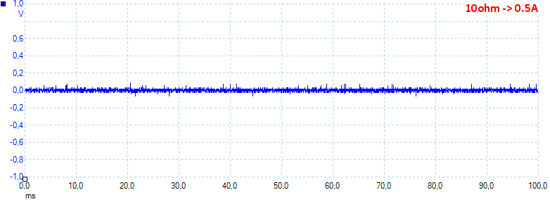
At 0.5A the noise is 15mV rms and 175mVpp
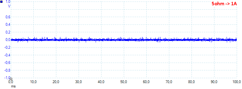
At 1A the noise is 18mV rms and 178mVpp
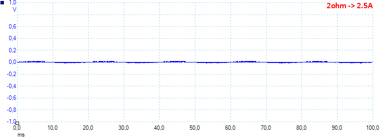
At 2.5A the noise is 12mV rms and 112mVpp
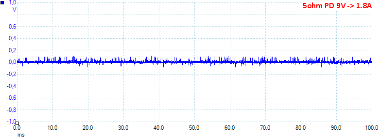
At PD 9V 1.8A the noise is 16mV rms and 220mVpp
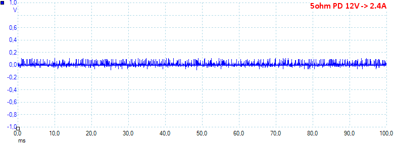
At PD 12V 2.4A the noise is 19mV rms and 205mVpp
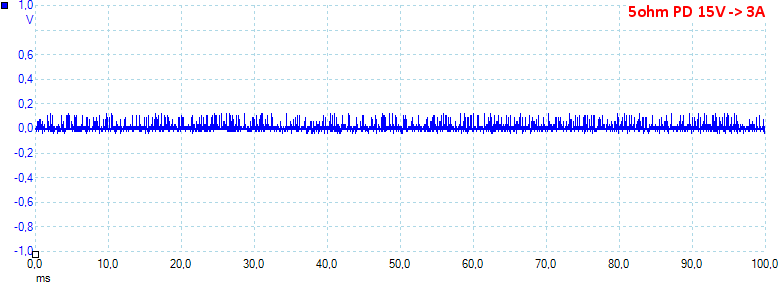
At PD 15V 3A the noise is 29mV rms and 252mVpp
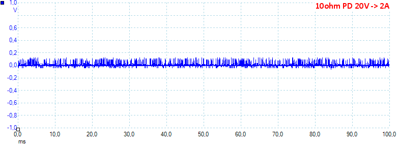
At PD 20V 2A the noise is 22mV rms and 202mVpp, all curves show fairly low noise.
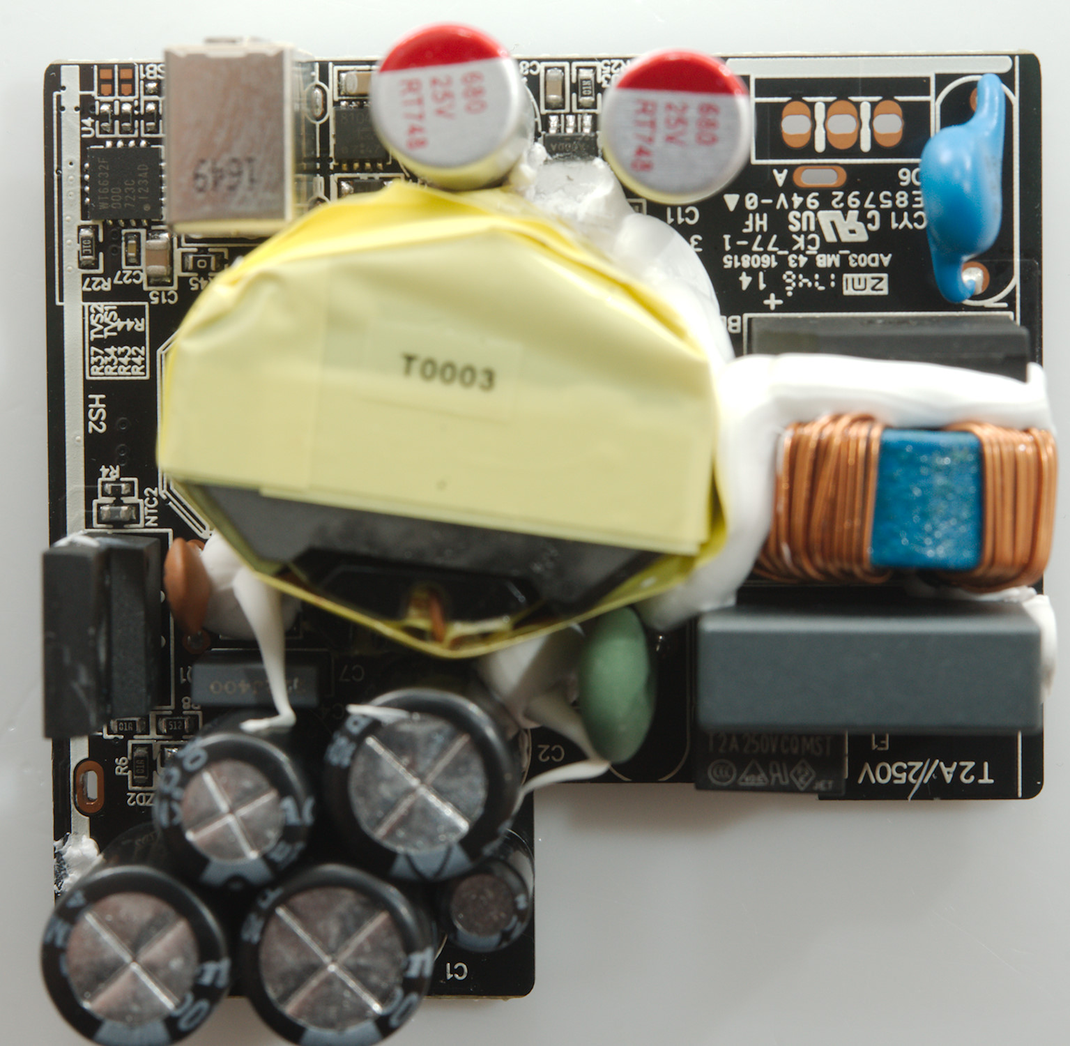
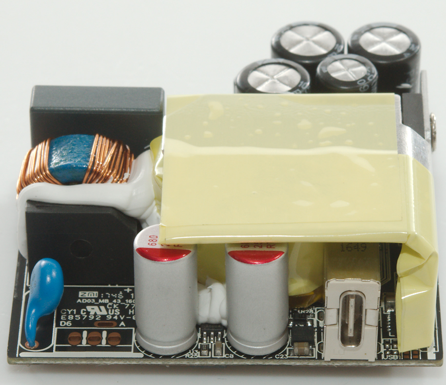
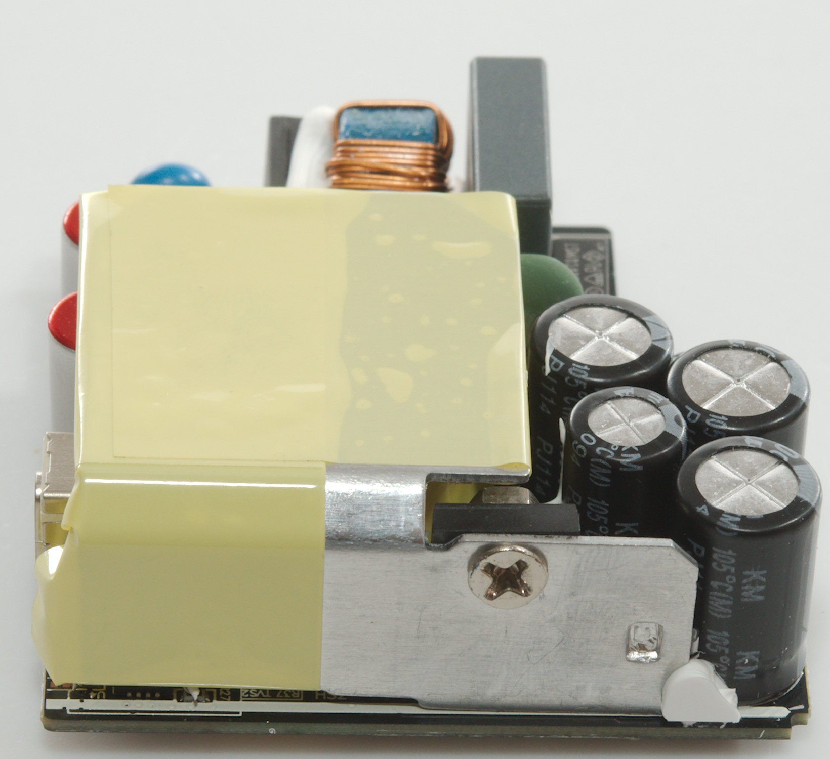
Tear down
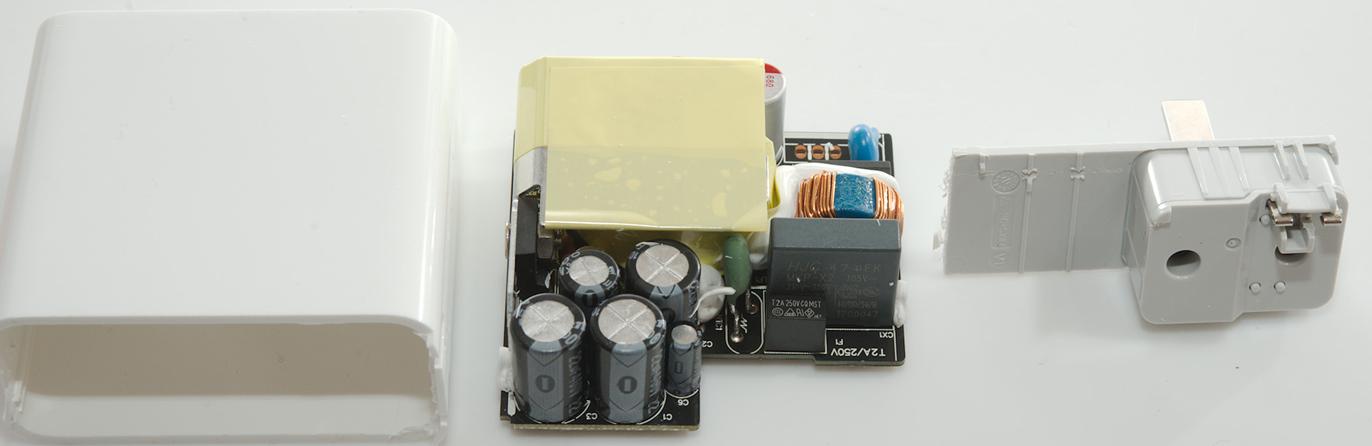
It did not look like I could open it with my vice, so I decided to cut it open.
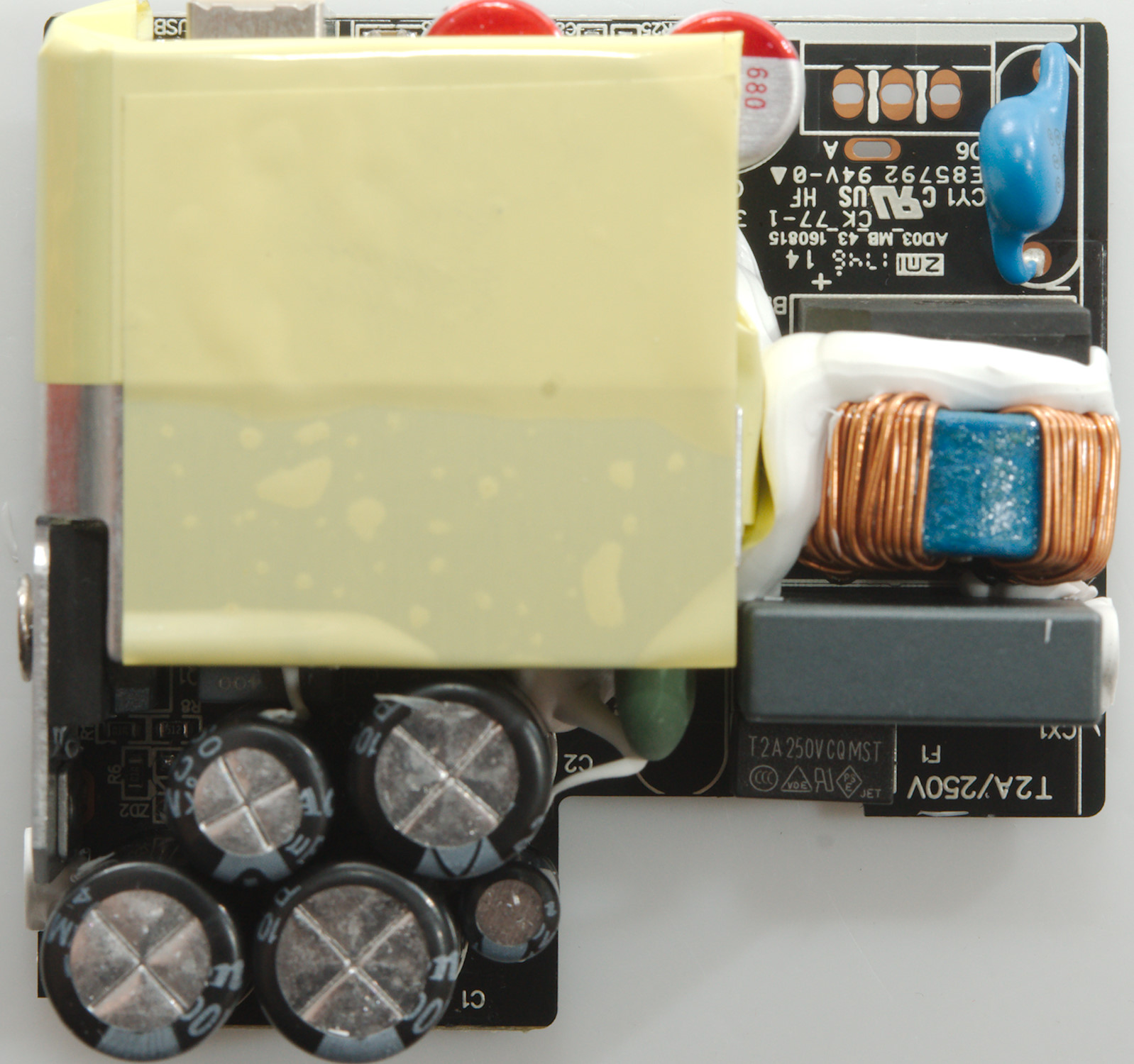
A heatsink covers a large part of this side of the circuit board, it is mounted with one solder connection and screwed to the main switcher transistor. The yellow tape on it provide isolation to the low volt part of the circuit board.
At the mains input is a black fuse (F1: T2A/250V) and a inrush current limiter (NTC1). There is one common mode coil and next to it the bridge rectifier (BD1) and the safety capacitor (CY1). The mains smoothing capacitor is made up of a couple of capacitors. The mains switcher transistor (Q1) is at the edge of the circuit board.
On the low volt side there is a 6 pin synchronous rectifier controller (U3), next is a power mos (Q4) to turn the usb output on/off and at the corner is a usb PD controller and more (U4: WT6632F).


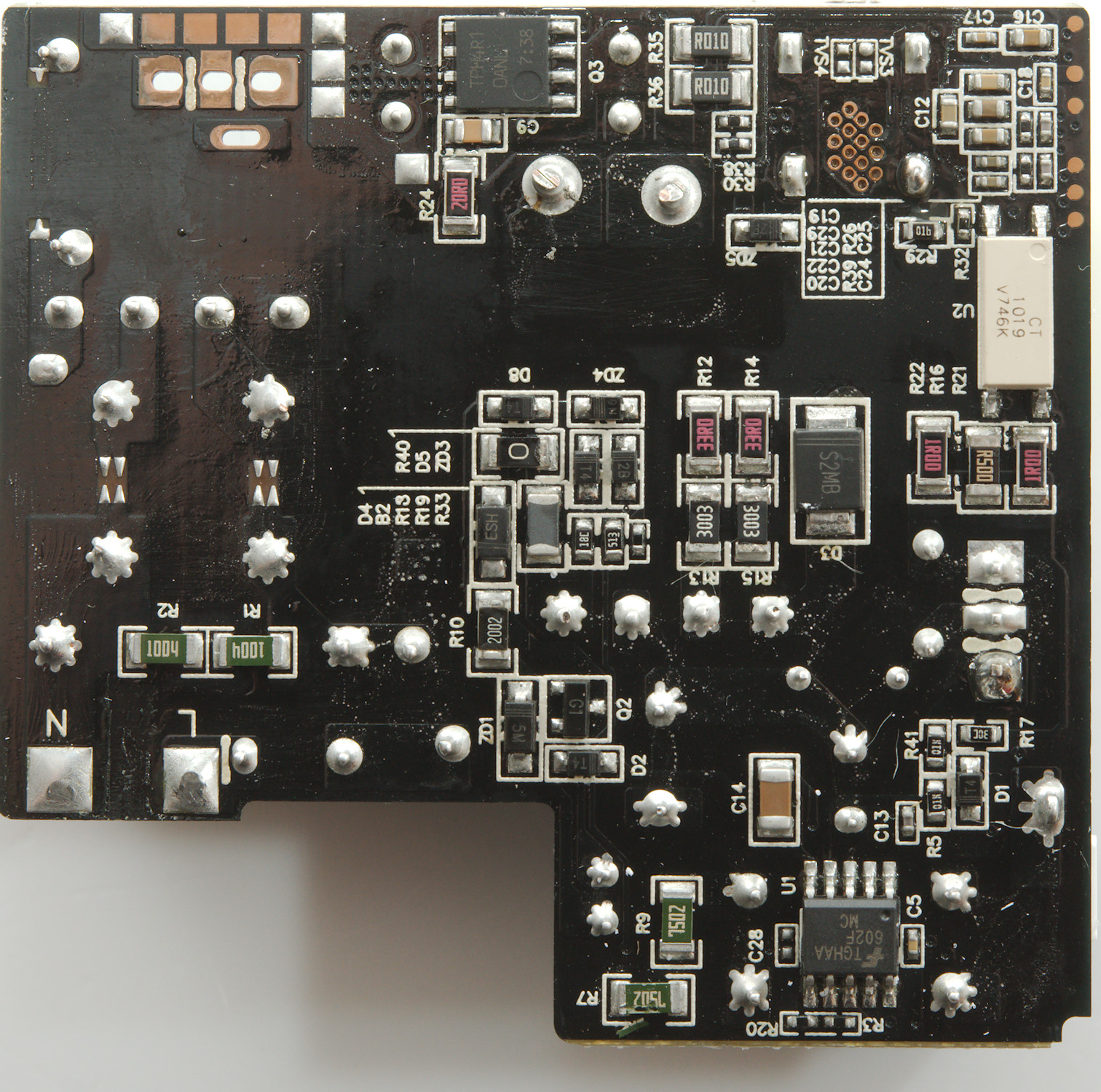
This side has the mains switcher controller (U1), a very long opto feedback chip (U2) and the power mos for the rectifier (Q3)
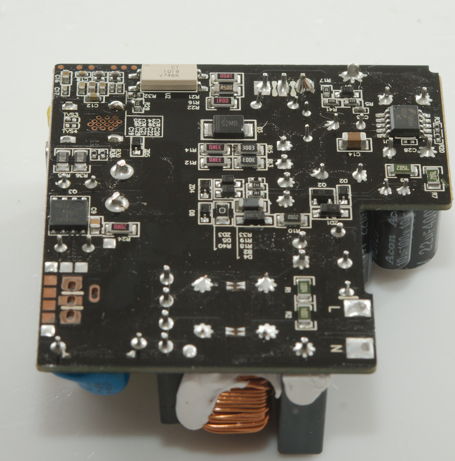
The distance between mains and low volt side looks fine.
Testing with 2830 volt and 4242 volt between mains and low volt side, did not show any safety problems.
Conclusion
With 45W this charger has enough power to charge just about anything including laptops, the output voltage is very flexible and as a added bonus it can also do QuickCharge. The noise is acceptable and the safety looks good.
I will call this a very good usb-c power supply.
Notes
Read more about how I test USB power supplies/charger