Need Some Help Troubleshooting Own (Partially Working) Design - High Efficiency, Small Footprint Boost Converter 6V 5A Driver

Hello everyone. I’m an electrical engineer from Spain who recently got into the flashlight world and decided to try and design my own LED driver. I wasn’t very happy with some of the fixed current driver designs out there and that’s why I went for a boost converter configuration: From a single LiIon cell input to 6V LED output (or two 3V LEDs in series).

As explained in the title, the design is divided in two parts: The boost converter itself (which is completely working. I’m able to get up to 96% efficiency from it) and the control loop. I wanted to control the converter to get constant current instead of constant voltage: In order to do this, I substituted the simple voltage divider going into the feedback pin of the boost converter for a current monitor + amplifier. This way, I can read the current at the output of the converter, and transform it into a reference voltage that I feed into the boost converter IC feedback pin.

Here’s a picture of both PCBs. The big one being the boost converter, which works fine when I use a simple voltage divider made of resistors. The small PCB is the current loop. The potentiometer controls the gain of the current loop, which allows me to vary the output current of the driver.

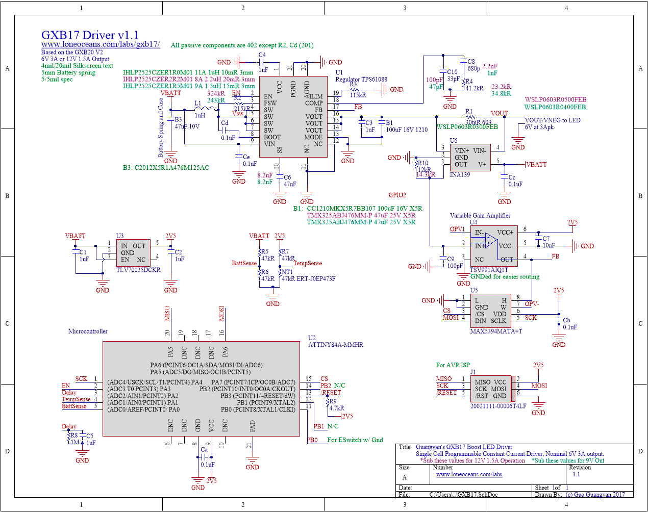
Here’s the boost converter schematic. It’s based around the boost converter IC with integrated switch TPS61088 from Texas Instruments. In the datasheet they state that the feedback pin should receive a voltage of 1.212V coming from a voltage divider between the output pins.


Here’s the current loop. I use an INA250 as current monitor (due to the super low, 0.002 Ohm integrated shunt resistor), a TLV8811 OP Amp to amplify the output of the current monitor, and finally a TPS71728 linear regulator to keep an stable voltage for both the current monitor and the amplifier.


As explained, the driver board, when used with a voltage divider to give the voltage reference to the feedback pin, works like a charm. I get a stable output with no noise, perfectly stable across the whole input voltage range. The input voltage is also noise free, both when using a battery or a laboratory bench power supply. The efficiency is also always above 90% from 0.001A to 4.5A.

But when I try to control the output current with my current loop PCB, that’s when the problem starts: For the same input and output voltages, and same power consumption, the output is constantly oscillating and I get tons of noise on the input voltage as well. The average output voltage and output current are more or less where they should be, but the efficiency drops to 60%, the feedback loop starts to oscillate… It’s just a mess. Here is an oscilloscope capture of the input voltage (yellow) and the output voltage (blue). Note how the input voltage gets a nasty oscillation when the output voltage rises every cycle. The circuit itself also starts making sound at the switching frequency (when controlled by voltage, the oscillation frequency is way over the human hearing limit, but when using the current control, there cycle happens at around 500~1000 Hz).


Here is another capture of the input voltage (yellow) and the feedback voltage produced by the control loop PCB, which is fed into the FB pin.


Is there an obvious mistake in my design? Why does the whole thing oscillate like that instead of giving an stable output like when controlled by voltage?

It would be very appreciated if you could post your thoughts or questions, so I can solve the problem and iterato on the design to make it even more efficient.

Thank you in advance for the help!

At first glance my guess is that the op amp is going unstable and ringing. This could be due to the gain set too high or lack of feedback or a compensation network.

But i haven’t reviewed the datasheets yet.

[edit]
Which INA250 are you using, A1—-A4 ?

The TPS chip has internal sensing of the inductor current on the input side, and it switches the internal FETs as needed to stay under the limit.

i think your current loop is trying to measure the output load current and feed this back to regulate current. It may be that these two current controllers are getting into a mode to fight each other and cause the oscillation.

[edit2]
The tps datasheet indicates that the FB pin is used to set the output voltage; you are trying to use it to regulate current. The maximum current limit can be set by the resistor value on the input of ILIM.

With your circuit changing the FB signal, then the voltage will have to oscillate as it tries to create the constant current that you desire—that is how PWM works. Have you measured the load current, is it constant?

[edit3]
deleted

I’m using the A2. I calculated everything to be able to go from 0.05 to 5 A

I thought about that too, but while researching for a similar design to review mine, I found this design from a fellow forum user. It’s practically the same approach, but he’s using different chips for current measurement, OP Amp and LDR (check the right side of the picture, that’s his current control). That’s why I think that it should be possible to control it by current. According to his blog post, he got very stable results: GXB20 - Single Cell 20mm Boost LED Flashlight Driver

Can you see any big difference?

You may want to look at control schemes on some of his newer designs, which use an op-amp as an error amplifier given a current sense measurement and a current setpoint reference voltage as inputs, and which feeds a control signal to the FB pin using a current-injection adjustment method. Simple and easy to stabilize.

The output frequency is pulsing at about 350 Hz, which is due to the L/R of the inductor.

The op amp is being driven to the rail (2.8V) by the high gain in the negative feedback.
after your explanation below

You left MODE floating so it’s using PFM, not PWM in light load condition. Not sure if that matters, but its different.

How could this be solved? Could you elaborate a little bit more?

If it wasn’t oscillating, the whole circuit is calculated not to go to the rail voltage. It should be always within limits. If I use the feedback loop alone, it’s able to generate the FB voltage correctly for the entire range of current (0.05 to 5A).

What I would need to find is the reason why it starts oscillating like that (or if there is a way to stop it).

I tried with both modes, but it doesn’t change the oscillation. It’s just as bad :confused:

Was the oscilloscope trace taken unloaded? or what is your load and the output current corresponding to those traces. At what location on the schematic were the scope probes attached?

What was value of RT used to set the switching frequency?

The ratio of inductance to resistance, L/R, of the inductor can be used to determine the maximum frequency that current can flow thru the device. The slope of the output voltage rising in your scope trace is exactly that of the rise one would see in an inductor with nearly the same time constant as the inductor in your circuit.

The TPS chip is turning on the low side FET to get current flowing in the coil, then at the peak current it switches the current to the output path (hi side FET) to charge up the output voltage. When it reaches the desired Vout then the FB signal will exceed the reference set point voltage (1.2v) and trigger of the FET. After a short delay it begins the cycle again. So that is why we need to know the RT, to know the switching frequency and determine the impedance of the inductor.

By your schematic the pot is adding 500k in the leg back to the inverting input of the Op Amp which will cause its output to drive to the rail. i see now how you are using this.

To hold 6V output, your circuit must feed 1.2 V into the FB pin when the output is 6V.

i’ll check back tomorrow.

All the tests were done with a HXP50.2 LED (6V) attached to the output. As commented earlier, I did the same tests first by using a voltage divider (A simple potentiometer between Vout+, FB and Vout-) and went from 0.01 to 5A output current (measuring with a current clamp, by sweeping the output voltage from 5V to 6.5V approximately to get those currents on the LED), and then did the same tests with my current loop PCB (same current for the same voltages, as they are determined by the LED). When using the voltage divider, the output voltage and current were very stable and flat. There was no audible noise (I’m guessing the audible noise is created by the low frequency oscillation caused by my current loop, which turns the output and input crazy).

The probes at the input were directly attached to Vin+ and Vin-
The probes at the output were attached to Vout+ and Vout-
The probes at FB were atached to FB and Vin-

Here’s the boost design alone (I used another cap to have around 10ms of soft start, but the other components are the same).
As you can see, I used 412 KOhm as Rt

Regarding this, I first tested the current loop PCB by itself, by creating a known current and making it flow through it shunt, in order to see that the current measurement and the amplification stages worked well, which they did. The values made sense (by sweeping the pot, I get 1.212V from 0.05A to 5A).

I think it’s also important that I mention that I created a second control loop PCB and tested it as well, but got almost exactly the same result. It’s the same working principle (same LDR, same OP Amp in non inverting configuration), but I’m using an INA138 + shunt instead. When measured with the oscilloscope, the input and output response/noise was nearly the same as the other design. That’s why I chose to just work on the INA250 control loop design that I posted at the beginning of the thread.

Here’s the second design I’m talking about:

Thank you very much for your time and help!

If there is any measurement that you would like me to do, I have time today to go to the lab today and do it, just in case that helps.

First some observations based upon the circuit values.

The switching freq is about 400kHz based upon the RT value of 412kR; the reactance of the coil is about 6.7 Ohms at this frequency; the coil L/R time constant is about 1 msec.

the input current limit is ~ 11.3 A based upon the Rlim of 105kR; the compensation network RC time constant is 62usec.

Looking at the scope trace.

The output is rising and falling at about 400 hz, which corresponds to 3 time constants to get up and 3 to go down, for the coil L/R.

The high frequency ringing during the rising slope on the output and on the input (yellow) is about 31kHz, this is a period of 32usec and way above the threshold of hearing. and half period of usec, which corresponds to the RC filter of the compensation network. It appears that the switching of the low side FET is pulling down the input power supply during this ringing.

The FB value is only correct at one setting of the Pot for a desired output voltage and current setpoint.

At lower output levels than the set point, the FB signal is too high and causes the TPS to shutoff the high FET; then the cycle repeats and turns on the low side FET.

Possible culprits:
The compensation network and high current limit seem to be beating against each other trying to control the TPS to reach the set point.

Or the Vcc is not holding up and causing the 2.8 supply to fall.

Here’s a measurement with the scope—see what Vcc is reading while running with your current loop/Pot circuit. Is it holding up or does it drop out? What about the 2.8 supply also?

Here are the measurements for 3 different output voltages/currents, from low to high.
There is always one picture with several cycles and then I zoomed into one cycle.

- Yellow is Vin (Vin+ and Vin-, which are also Vcc and GND in the current loop board)

- Blue is Vout (Vout+ and Vout-), which are connected directly to the LED

  • Violet is the LDR output (in other words, the 2.8V output and GND)

In all of them there was audible noise, exactly the output frequency

Low intensity output:

Medium intensity output:

High intensity output (the pot is turned almost all the way):

Hi SZapatero,
as sidehack pointed, loneoceans used a different design on his later drivers, you may want to try.

His later drivers blog entries lack a scheme, but the same implementation can be seen on other drivers on this thread:
https://budgetlightforum.com/t/-/46129

To save you work i´ve made a scheme i hope is correct:

EDIT: With this design you need Rfbt y Rfbb resistors, like in the boost scheme on your #8 post

Those are some great scope captures, and it shows how the supply Vin is being pulled down when under load. It’s not so bad at light load, but really lays down at the high intensity output. Either the battery cell or your power supply is not up to the task of supplying 12A at 4 volts. When it folds it takes the 2.8 supply down with it and then you lose the INA and TLV op amps and the FB signal too.

You might try changing Rlim to decrease the input current limit to something lower, e.g 5A, try 240 to 300k, and see how it behaves. This might fix the ringing issue, or at least provide some improvement.

i thought you may have been using the Vcc pin on the TPS61088 chip as the source for the Vcc on the Current Loop Board since they had the same reference designator, and that was my suggestion to monitor the Vcc output pin of the TPS61088 chip to see when it collapsed. But the 2.8 collapse is really the kiss of death and shows it. The output Vcc may show it earlier.

[edit] Found the UVLO section

Here is the functional block diagram of the 61088 chip and my guess as to what is happening.

Notice the comparators for the current limit and the FB signal that are OR’d into the set-reset flip-flop. The low side FET will turn ON and stay on until one of those comparators goes Hi, which means that either the Input current hits 11Amps or your current loop indicates the Output current has reached the set point as adjusted by the pot. i doubt that the input current is ever hitting the Clim, so the Low FET is causing the battery or power supply to be pulled down so hard to upset the UVLO and 2.8V supply.

TPS61088 FBD

I also think that this might be the problem, and not Clim, simply because the problem with the power supply getting pulled down happens even when the consumption is still very low (2A input current). Also, the audible noise happens throughout the entire spectrum of currents, whereas with no current control, the converter is dead quiet all the time.

These tests done on Saturday were done with a decent lab bench power supply, but some days ago I tested the design with some very current capable Li-Ion batteries that I use specifically for spot welding, and they are supposed to be able to deliver pretty much any current.

I’m going to try and get some scope captures with this batteries as soon as I can.

My thought with changing Clim with a different Rlim is to get the Deadtime Control Logic to switch sooner and send more current thru the Output path.

If neither the input current reaches 11 Amps nor the output current reaches the set point level of your current loop board, then the flipflop logic will not be reset to turn OFF the low FET—it will stay ON and pull down the supply.

Due to the reactance of the coil, i don’t think it is possible to get 11 Amps at the 400 kHz switching frequency, so the Logic Reset due to Clim is not happening. If the device would release the Low FET sooner then current could flow thru your current loop board and raise the FB quicker and get into regulation.

As it is right now the FETs are OFF most of the time as current flows thru the diode of the High side FET, seen in the Output voltage decay. When this current falls off such that FB drops below the hysteresis band, then the Low side comes back ON in an attempt to pump up the coil, but the high current limit is impossible to reach. The low intensity test may actually be operating with FB causing the reset and it is not disturbing the 2.8 supply. The second scope trace of the low intensity is my favorite to see the low side pull-down and FB reset.

If you can repeat your low intensity test and remove the 2.8 signal, but add the 61088Vcc and FB signal to your scope trace it might show Vcc being pulled down but not past the limit, and show FB moving with the output current.

Hello SZapatero,

Welcome to the world of power electronics where I see you have made an introduction with some tricky aspects in this field. :) Thanks for all your effort with the detailed documentation of your project! I also appreciate how methodical you were in splitting the system into two parts and debugging them in a very systematic way.

It's difficult for me to debug in detail what the exact root cause of the circuit you have is, but it's clear that you're experiencing some oscillations - this is very common in any system which uses feedback. From the get-go, I already see some flags - any of which could possibly cause a problem, but likely they're all interacting in some way and contributing together and it's hard to say without examining each part in detail. Here are just some of my guesses from what I can see.

Let's look at layout and schematic. At a high level, the schematic looks OK, but there are some aspects that you could try improving about the layout, especially the interface between the two systems. For example, the feedback line from your current amplifier circuit to the boost converter has a very large ground return loop; this adds a bunch of inductance to this very sensitive analog signal and it's going to be picking up all sorts of switching noise (+ground bounce) exacerbated with extra loading on the output of the op-amp. Ideally I'd have both circuits laid out on the same PCB with care to ensure a good low impedance and shielded path for this line. For now, you can improve it significantly with a twisted pair (together with ground) going from your amplifier board to your Boost board (I see you have an extra GND pad there already).

Next, component selection. The TPS61088 regulates based on a cycle by cycle basis using the internal error amplifier, in your case, around 400kHz frequency. Typically with a resistor divider, the feedback pathway goes directly from the output to the internal amplifier with no additional delay. By adding current-based control, you add a whole bunch of amplifiers in the signal pathway. Now imagine if these amplifiers do not have a sufficient frequency bandwidth to 'react' quickly enough to the output, you can start to see how the regulator may go out of control and begin to oscillate.

Think of it this way, let's say you're trying to push someone on a swing and to keep them at a certain swing angle (regulation). Each cycle, you use your eyes (the feedback) to see where the person is, so you can decide how high they are, and how hard to push, at what time. Now imagine you're now looking at this person through a video camera, but this video camera is super laggy and feeds you either a delayed video feed or one with a very low frame rate... it will now be very difficult to control the output (the push you give the person on the swing) to regulate the result. You will want a video camera with as low a delay as possible with as high a framerate.

Browsing the datasheet of your two main amplifiers - the INA250, and the TLV8811, I'd like you to take a look at the datasheets of these two component, as well as the frequency bandwidth of these two components (especially your op amp), and compare them with the general operating frequency of the TPS61088. You can also compare them with the components I chose for my circuit previously. These two could be affecting the performance of your circuit, or maybe just one of them, or both, in addition to other aspects of the system. These are just some of the things I saw, but perhaps there are more tricky bits we may have missed.

Good luck!