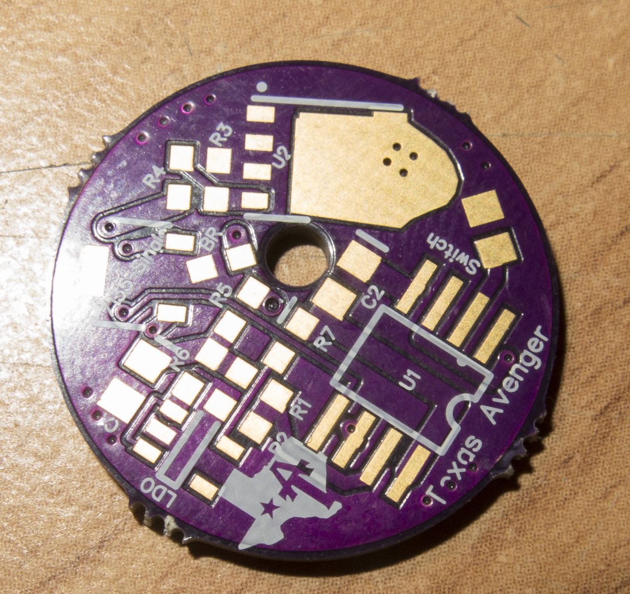
Strange you're having issues with that driver. Yes, it is the "old configuration" with the capacitor after the diode, but I have built and sold hundreds of these without experiencing that issue. Tom has used them as well, even souped up if I recall.
Well i have to try next time with batteries before making any changes to make sure it is not failing because of my lab power.
But after moving C1 before D1, it has been working nice. Very good board thanks!
I’m learning how to use Eagle now and i was thinking to try draw SRK board with 3-4 7135’s groups so i could use without PWM, or maybe one 7135 with PWM, for best efficiency. Is there really sense, maybe not. ![]() After that there is ofcourse problem with firmware, don’t know if someone has done that already.
After that there is ofcourse problem with firmware, don’t know if someone has done that already.
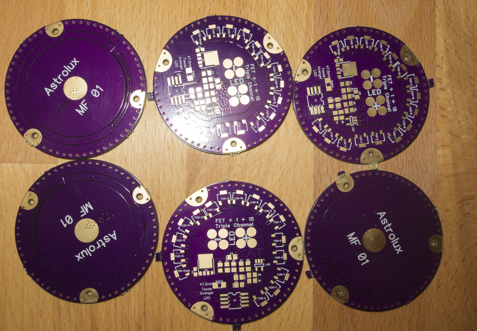
You might check out some of the new triple channel drivers and firmware before designing your own Oshpark board.
Sure, i tried to search but couldn’t find any triple channels, can you point me where i could find some?
Still i would like to learn Eagle (and better coding), have to try something and order and see what made. ![]()
I don’t know how i didn’t saw that there was really three channels used in that code and pcb, but yes, there really is. Have to say this looks really awesome, Texas_Ace has done really huge work for this driver!
4 parallel 18650 battery plates. I’ve searched and cant find anything. does anyone know if they exist or even a battery carrier the ends can be robbed from? This is for the Ol comp light build.
Steve - Can you salvage them from a cheap SRK? Might be cheaper overall.
Thanks Tom. I would if I had one. Wonder what the cheapest 4 cell torch out there is?
Think about $14 US. Let me check my order history in Ali... 
here it is: https://www.aliexpress.com/item/High-Power-3t6-LED-Flashlight-Torch-3-14t6-3-x-XM-L-T6-34000-LM
OSHPARK says there must be a 15 mil clearing between traces and outline. Shouldn’t this also affect the ground ring on our flashlight drivers? I have checked a couple of board designs from forum members and have NOT seen this clearance anywhere. Isn’t oshpark that strikt with its design rules, or did they correct the gerbers or what else?
It is hit and miss, sometimes they cut the copper back from the edge of the ground ring and sometimes not. I always have it extend to the edge and if they cut it back, so be it.
On driver that are really tight you can oversize the pcb and sand it back to make sure there is copper to the edge.
Thanks. I’’m working on a Q8 driver currently and actually there is a tight fit from tube to board, so I think I have to do oversizing and sanding.
Btw I also had a look at some of your drivers and noticed you use a clearing of only 8 mil between ground pour and other signals. Have you ever experienced faulty boards because of this or did they all work out ok? And - as far as I could see - you don’t enable thermals for your ground pour - is soldering still easily doable without thermals?
I use whatever the specs on oshpark are as the tolerances on my drivers, unless they changed recently that is. I always run the clearance test to make sure everything clears before releasing a driver. Never had an issue yet.
All my drivers are setup to be hot air reflowed, so the whole driver is heated and reflowed at once. In this case the thermal setup of the driver doesn’t effect the soldering a lot. Never tried it with an iron nor would I even try to do such a thing to be honest.
That’s good to know, thanks again.
Oshpark wrote me the solder mask should no exeed 30 mil beyond the board cutout to not make problems in the fab, TA boards are copper poured to the board outline and so far all boards I ordered over 200
the bigger ines have copper till to the edge, but the small not, not sure why
just too wide solder mask of the 46mm and 21, 22mm LDO had problems the fab removed the outer solder mask ring as they hit boards around
On one fab ground rings were not removed, but the other made problems
I’ve already read your former post (I guess in TA drivers thread) regarding this solder mask problem. Very helpful, thanks. Do I understand right: only the solder mask above the outer copper trace has been removed, and not the copper trace itself?
The copper pour on TA drivers is matched to the board outline, of course it would be possible to manually widen it over the board outline, question is if its working
for solder mask
The Gerber files contain a ring shape that was on some drivers a few mm over the board outline
in one fab that collided with boards around it so it was automatically removed on the panel, so the copper ring was there but fully covered with solder mask
I try this experiment in one fab
copper pour and solder mask expanded beyond the board outline
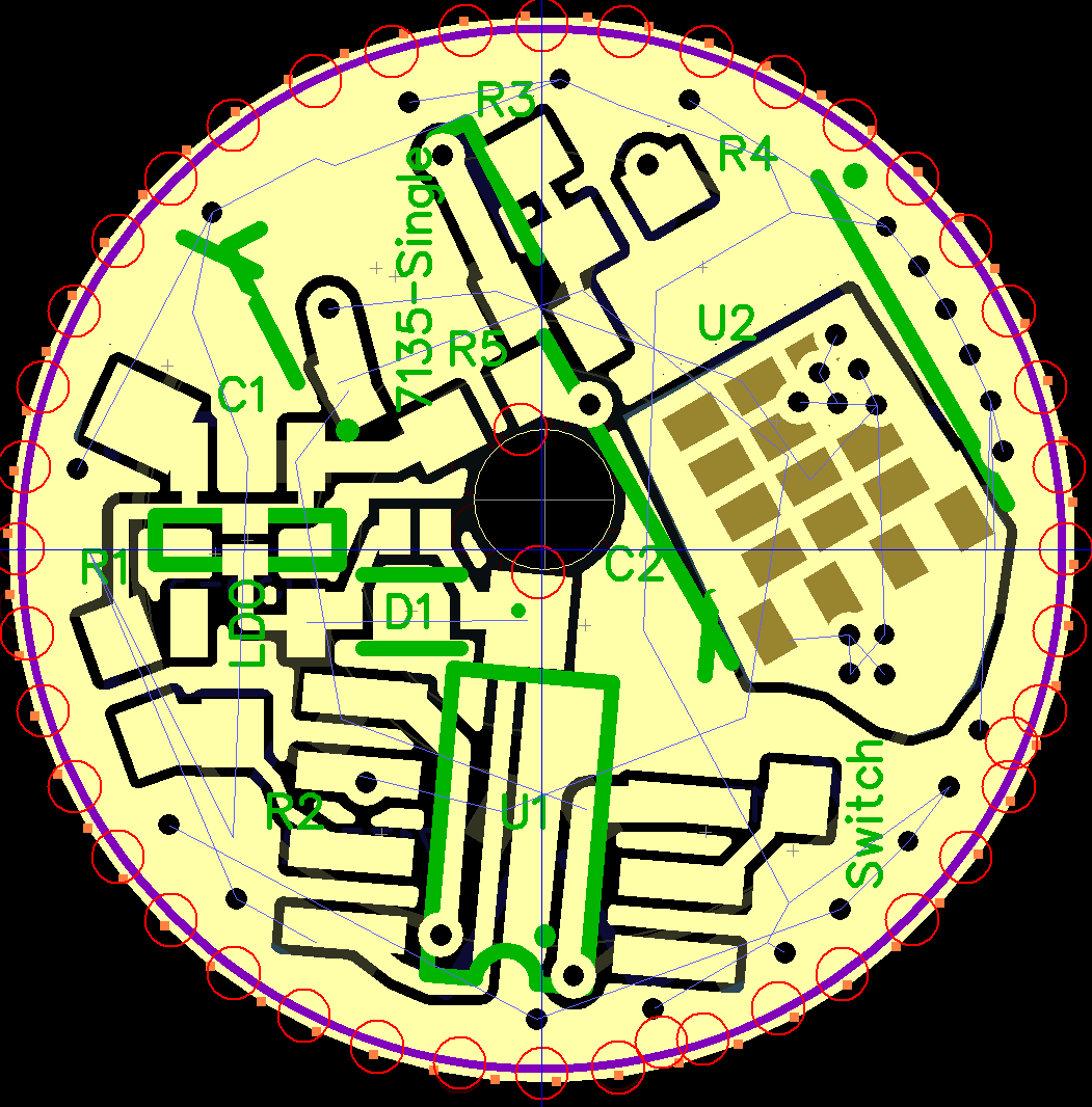
I like life to be predictable. So all my boards are made within OSH Park design rules. I design all my boards to be bigger diameter to make up for the copper-to-edge set-back required. Then, they are ground down to the edge of the copper pour. Some people have gotten by with designs that had copper all the way to the edge. But sometimes (maybe now it’s all the time) OSH Park will set it back themselves. In some cases, that can make the board unfit for its intended purpose.
I lost all my eagle stuff when I moved to linux
Can someone create and upload a 17mm to 20mm adapter board for the BLF 17mm driver for the new type C8 lights