Mike C asked me to share the libraries I used in EAGLE to design my first attempt of the 17mm board,
so here are the devices I created myself: My Library
If you need the ATTiny84a footprint as well, I suggest downloading the Sparkfun library here: Sparkfun Library
If you want me to design the MAX5424 as well, just ask for it
loneoceans: When you have made these boards, have you used stencils or applied solder paste by hand? I have had a few shorts on MCU pins when using default MCU footprint for my 841 when applying by hand. The default mask pad size is bigger than the actual pin and overlapped with the other pins. I made it better by customizing the footprint so the mask pad size is exactly the same is pin pad size. However, I’m now using stencils I made with an even smaller cream pad size for the pins.
Laying out the board on 4 layers would certainly not only allow better performance but also allow better routing. However specifically avoided a 4 layer stack to keep the PCB costs as low as possible. Adding blind or buried vias significantly increases cost so I usually try to avoid them as much as possible. I'll explore a little with the 17mm version when I have time though it looks to me that there should be no problems making a 2-layer 17mm version.
I didn't bother fabricating a stencil for this since I was expecting to only make a very small number of boards, so I soldered them all by hand with a combination of reflow and solder paste applied by hand using a toothpick (typically I don't get any bridges if the right amount of paste is used, or I fix it using solderwick), and solder the rest by hand under magnification with a tiny tip soldering iron. Like you mentioned soldermask expansion needs to be adjusted. I think I used 1 or 2mil expansion, depending on the fab I go with.
Yes it will work just fine with some small adjustments (e.g. to make sure it doesn't try to drive 9V at 3A, adjust components to make it more efficient st the desired drive currents etc).
I have run them up to 12A and they still worked fine. Check my sig for a test of them, they didn’t even reach peak lumens until ~6A. Although around 4-5A is ideal IMO.
Besides heat from the LEDs, running at 3A at 9V output is also impractical from a single 18650 cell drive in most flashlights as well. The 27W output will require at least 30W input or more, which for most 18650 cells will require about >=10A input current which will be just about too much for the driver to handle safely. Contact and switch resistance will also lead to significant losses. However, 9V at 2A or so is completely OK (at least for the GXB20) :)
I didn’t see this in the OP. Curious what are the limits of this driver when it comes to power. I assume that the true limits lie in the input current?
I assume this could boost power to an 12v XHP35 as well with some component changes, what kind of output current would be possible?
Also, did you ever say what components you are using for this driver? I never saw a parts list, curious what boost IC you are using along with the rest of the parts.
If this could be shrunk to 17mm an xhp35 S2+ could be a really interesting EDC light (or xhp50.2 for that matter).
A TPS61088 is used as the boost converter, here is the website, even with a schematic: loneoceans labs | GXB20 v1 LED Driver PCB
I currently try to get it shrunk to 17mm (with a few modifications to the circuit).
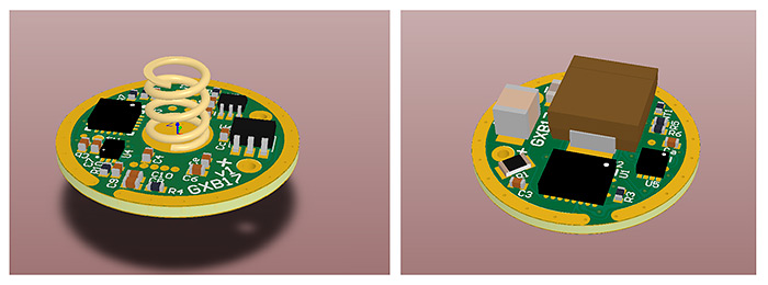
Very soon! Layout for GXB17 is basically done. Just need to order a few PCBs and to fine tune everything (render above is not final yet, was taken during initial design). The hardest part is designing within the 6/6mil constraints of OSHpark and using 2 layers with no air-wires, though I've fabricated 5/5mil with them and they seem.. just fine. I suspect even 4/4mill will still be OK!
There are several aspects to the limits, but not hitting on the more nuanced ones would be the maximum input current of 10A. In addition, making the driver efficient at different output / input voltages requires fine-tuning the component choices such as the switch frequency, inductor and error compensation network - i.e. one cannot just run the driver for a different output configuration while expecting similarly high-efficiency output. However, if one is willing to sacrifice a bit of performance, then changing it should be fairly straightforward.
I'm still in the process of writing up a page for it but my 'sales' page has a decent overview of the BOM and Schematics. http://loneoceans.com/labs/sales/gxb20v1/ Note the V2 version is fairly different with some enhancements.
Finally there are obviously other limits to the other components such as minimum voltage input required for proper operation, thermals (getting pretty warm already at ~18W output) as well as boost inductor. Trade-offs I suppose between cost, size, efficiency, performance and features :)
So it is setup for a 7A input, thats pretty darn good. What is the limiting factor? I see the inductor is rated at 11A but didn’t take the time to look up everything else.
With a 7A input limit, that would be around 1.75-2A to an xhp35, which is pretty darn good. If it could drive it a bit harder to 2.25 - 2.5A it would be perfect.
Yeah, heat buildup should be the limiting factor, the question is which component? If you stuck the driver with thermal cubes you can usually get some more out of it if you know where the heat is coming from.