If you do that, instead of 1+2+5, I’d suggest doing 1+1+2+4 — with PWM only on the first 1x7135 channel. It lets you do a no-PWM level every 350mA. As an added bonus, instead of using 24 bits per ramp level, the ramp data can be condensed to about 11 bits per level, or 8 bits per level (plus 8 bytes and a couple extra lines of code).
That sounds like a good idea, but the boards are already ordered and shipped.
1+2+5+M was a compromise as I could reuse the existing triple-channel ramping code and just add a extra switch for the moon mode where one pin is set to low if the level is 0 and else is set to High-Impedance.
1+1+2+4 looks good if you have enough pins, but light and human eyes don’t really work in a simplistic linear fashion, so I think it is a bit of a waste obsessing about the lowest levels and ultra-fine precision (i.e. the 1+1 end.
I suspect you will be fine with 1+2+5, and a bit of PWMing on two of the lower channels. Which might fit with smaller MCUs that have limited timer-counters.
With the moon pin you can actually set two levels of moon. One high level using the pin pulled up hard (20 mA or more) via an external resistor to set a reasonable current, the other value using the internal MCU pullup resistor, plus anything external. This has been demonstrated and worked.
Except it seems better to pull the pins down, rather than up, to match the way that the main current to the LED is usually arranged. Never tried it myself.
Then there is the FET to deal with, which still seems to be expected.
The linear fashion was sorta the reason why I went with 1+2+5+M. This way I can have 1x7135 after connecting power, 2x7135 as the ramp ceiling and 5x 7135 as a turbo mode.
Regarding the two levels, I think you mixed up aux leds and the main LED. Aux LEDs (connected to GND and the MCU) can have high (pin set to high) and "low" (pin set to pullup)
But the main LED is constantly connected to VBat and the GND side is switched/regulated. In that case, I can only have one moon mode set by the series resistor.
I agree about the 1+1+2+4+8+16 (etc) approach being overkill, and not incredibly useful. I think it’s a pretty slick method though, and wanted to mention it since what you have is so close.
I’m generally happy with FET+1 or FET+N+1, or more generally, putting power channels about an order of magnitude apart. I haven’t found it very useful to maximize the number of no-PWM levels. And on ramping designs, swapping channels around has a tendency to create mismatched joints in the ramp, so I try to avoid that.
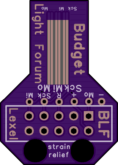
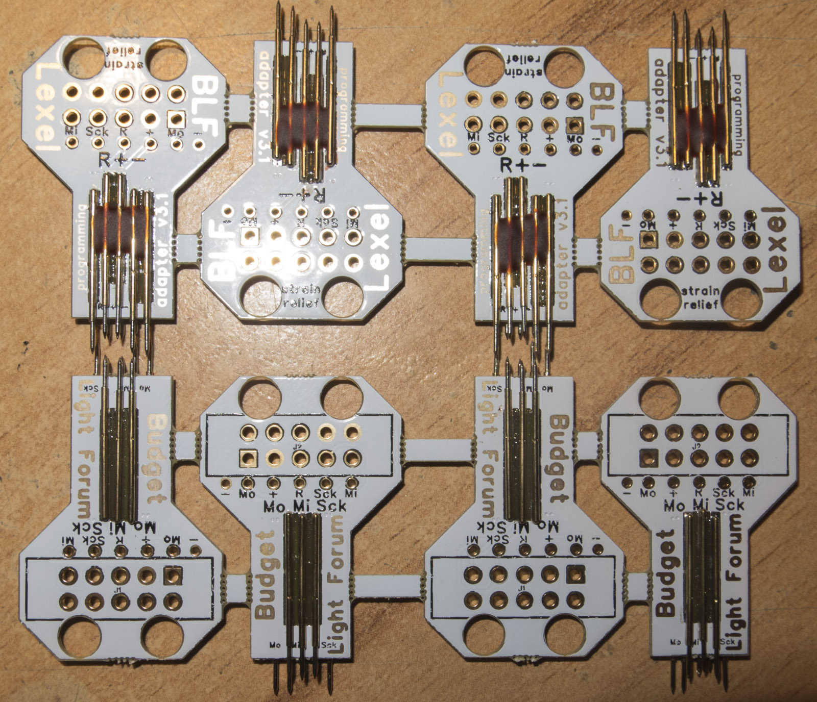
yeah just see I made the mistake not taking into account that the design program has vottom side mirrored
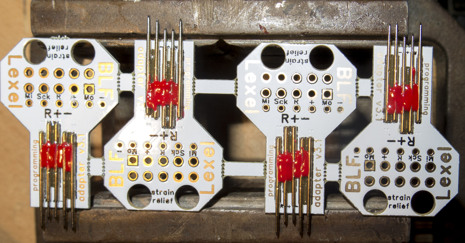
so the 10 pin connectors does not work 1:1, reverse 4 soldered leads should be no problem
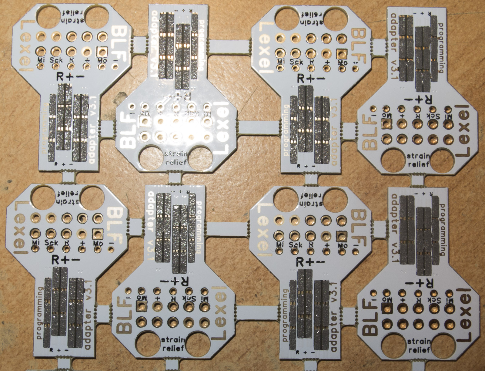
atm in customs with C8F 21700, MF04S, prototype D1S, D4, D4S, MF01 aux LED boards
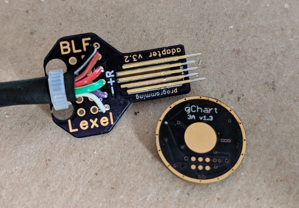
The picture shows a 4+4 key and the driver I was working on at the time I ordered the key. The DD+1 driver is 17mm and just there for size comparison.
The key-pcb is 10mm x 27mm, at the pogo-pins the pcb is only 5.6mm, that will fit about anywhere. When you only use 3x3, you can file the key even narrower.
Pcb width is 0.8mm. Pogo-pins are 0.68mm diameter, 16mm long. Via drills on the driver are 16mil (0.4064mm). Distances are 1.3mm between left and right vias and 1.5mm between up and down vias.
Just programmed a driver and it’s a hoot.
.
The size of the key is perfectly fine, can be put between thumb and middle finger with the index finger on top, gently pushing the springs of the pogo pins down. With 6 vias, aligning is of course a breeze.
Refined the key a bit, not much really. I’ll make at least two versions:
- A neutral one marked from A to H, where up to 4+4 can be used. With connectors any combination can be plugged on the fly
A key marked with the pin numbers of the Attinys in my preferred layout
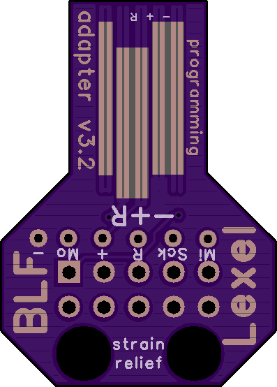
I also got my final revision 3.2 also launched now,
too bad I got made 120 boards here where the 10 pin header wont work and solder connection markings do not fit if want flash driver from bottom side
the pins are mirrored because I made an mistake looking in my program on drivers bottom which auto mirrors
Order in 2OZ for 0.8mm board thickness from Oshpark!
HarleyQuin and Lexel, do you have pinout and pcb layout recommendation for the programming pin connector? I think it make sense to standardize something for easy use on many drivers types.
I’ll give 6 pads a shot, though. Lexel, are all v3.2 fixed (not mirrored)? Or was the mirroring only on the 10-pin connector? I had trouble flashing this board (my first attempt at using your pgm key), but I think it was probably my driver design at fault.
Quoting this to say I’m still hoping somebody does a complete flashing kit that includes all the cables, plugs, clamps, etc. and this key. Convenience is a strong selling point for me. I haven’t started flashing yet for various reasons. Having a complete kit to buy from one place would knock out a couple of those reasons.
EDIT: I’d still want the kit to include the usual programming clip because I already own some drivers that don’t have pogo pin programming on-board.
If I want the key to be used on the bottom of the driver, do I apply the via pattern to the bottom of the driver or to the top of the driver? I want to get the mirror issues right the first time lol.
I assume it should be applied to the bottom of the driver since not all the patterns use vias?