Adventures in TinyAVR 1-Series

Yeah, sorry… I was referring to the ~$5 clones, like what is referred to in this guide

But if you’re going to use Atmel Studio (or compile avrdude on your own), then an Atmel dev board like the ~$8 416 Xnano is perfect.

Hwdef files do need modification, but that should be expected. It’s a different MCU, so a different layout.

Part of what I’m curious about /hopeful for… These 1 Series chips come with up to 32KB of memory. If TK can fit Anduril in 8KB, what can she do with 4x as much space? :smiley:

Hey…nice find with that jtag ice :slight_smile:
The best combination of simple and cheap that I’ve seen so far. :slight_smile:
Does it allow debugging 1 series chips or programming only?

Not that I’m aware of, though I haven’t researched that.

I have used the 416 Xnano to debug in Atmel Studio. That worked very nicely! You just disconnect the onboard MCU and then you can use it as a programmer/debugger for any of the newer chips (using the onboard mEDBG).

1+ for the 416-Xnano. Pros are that you can power the target with 5V from the Vref pin on the programmer side, has a CDC TX so you can talk with a terminal, user button and led, plus all the pins are labeled on the device side silkscreen, very nice and easy way to get going.

I also have the 817 Xmini, which is very nice but overkill if all you want is a programmer / debugger. Real nice dev board though. And still inexpensive.

Same here, if one is into it, not much trouble to get an Multifunctional Expansion Board Shield kit for the UNO to sit on top of that 817-Xmini.

It doesn’t sound like moving I/O between port a and port b is very hard so that’s good.

I once asked TK if she’d prefer to abandon the 85 altogether and just use a new one series with an adapter board but she prefers to keep the 85 for backwards compatibility. The amount of work she does to squeeze everything onto the 85 seems like a lot, especially for a volunteer. I’d like to she what she could come up with if she had IOT connectivity to work with.

How do you debug flashlight firmware in a board that does not resemble a flashlight driver at all?

You don’t need the LED driver circuit to develop the firmware. For most parts of the development an oscilloscope or logic analyzer is enough. Or hook up a small LED with a current limiting resistor to a free pin.

For initial firmware development and debugging, SammysHP hit it on the head. But also…

These Xnano and Xmini dev boards give you the ability to disconnect their onboard MCU. You can then wire the programming/debugging chip on the Xnano/Xmini to any of the 0-Series or 1-Series chips thru the 1 wire (plus power and ground) UPDI (unified program and debug interface). So you can actually debug code running on an actual flashlight driver.

Boy, I'd love to get into this development setup, if only I had the time. 32 KB is a whole lot, and would really like to see what can be done with 2 switches and multi-channel, multi-LED. If only I had more time.

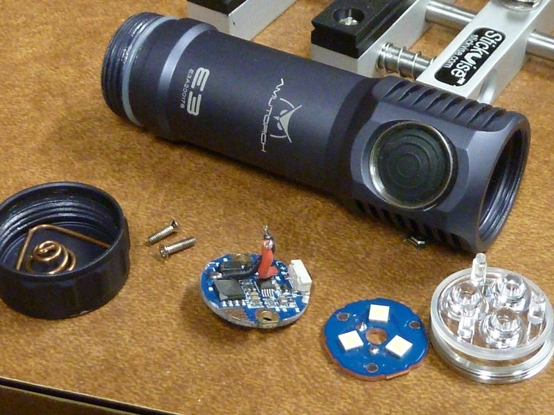
I got in a Amutorch E3 - 21700 triple LED, standard MCPCB, std triple optics. It's light weight and compact, but they made the cavity above the driver extremely small - 2.4 mm clearance over the driver, so I can't piggyback a small board in. Only option is driver replacement and it's got 2 screw holes for mounting - great idea really but no std OSHPark driver will fit, plus with a board mounted switch. Love to build up a OSHPark board for the E3 with this MCU.

Man, driver mounted switches can be a pain. Means you usually need a custom one-off driver. Got pics of the driver?

Actually CerealKiller did a OSHPark board with a driver mounted switch and I've used it a couple times. Not sure if I have pics - will take some and post.

This is one: https://oshpark.com/shared_projects/yoNxPZWi, this is his whole collection: https://oshpark.com/profiles/Cereal_Killer. I used this one: AT-008_V2

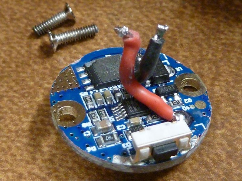
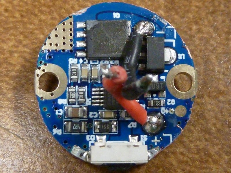
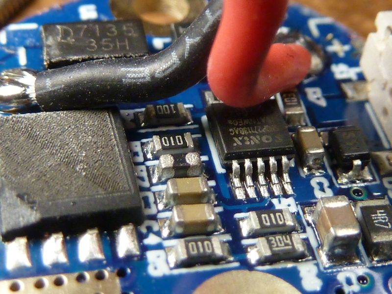
I already took pics but didn't post. It's a classic FET+1 design with the FET markings rubbed off, 10 pin MCU - not sure what it is, but here's the manufacturer's page: http://www.sonix.com.tw/category-en-947

Ohh, I do like how compact that looks. Appears to be a good candidate for a driver swap. Anybody have one of these that they want to get rid of? :wink: I wouldn’t mind putting a driver together for it.

Hhmm. Maybe you can have this one. Neal gave it to me, actually, with my last order. It's a one piece shell, but the switch is a bit squishy - too far off from the mech switch. I told Neal, he said he'd pass it along.

Naw, I don’t need you to let go of yours Tom. Half of the reason for acquiring one would be to put together a board you could play with!

Hi all,

thanks for sharing your ideas, I’m reading with interest what you are up to here and I might as well join in with a board or two.

It’s not that my wishes exceed the 85’s 8kB. I customized FSM/Anduril to my liking within 8kB, but I would very much like to have the possibility to have more resolution for PWM. Especially in the moon region and at the seams of the PWM channels.

If I read the datasheet right the 1616 supports more than 8 bit PWM, that would be THE argument for me to migrate.

I’m already converting a brd for a future project and like the idea of the 20pin 3x3mm versions best, hence my eye is on the 1616.

My next obvious question now would be: Which function at which pin? Where should the PWM go, where the switch pin, where the indicator LEDs?

Or does the multiplexer allow to connect every pin with every feature? And do all ports allow for higher PWM resolution? I saw gchart using port B (PB0-2) and adding the aux led on PA1, which I presume was more or less random. And which function would profit from the energy efficient Timer/Counter D (pwm, switch, indicator)?

I welcome your input. I got some spare time and I’m looking forward for some board design. But 600+ pages of datasheet is quite a burden for me, and I even did not fully fathom this multiplexer thing, yet.

Thanks
HQ

HQ, good to see you around!

Timer/Counter A and B are both 16 bit. Timer/Counter D is 12 bit. The advantage of using TC-D is the ability to have clocked separately from the main CPU clock. While it could have many applications, I feel like the main benefit for us would be to use the 32 kHz ultra-low-power clock for the main CPU and then we could still use PWM at a high rate without the CPU sucking up a lot of current. For the sake of comparison, say you wanted a 10-bit PWM (1024 steps) and a fast PWM rate (like 19 kHz). Using TC-A, the main clock would need to run at the full 20 MHz and the MCU would be drawing ~10.6 mA. But if we used TC-D and ran the main clock at 32 kHz, the MCU would only draw around 970 uA (less than 1mA). If we used this for moon levels, it could greatly extend runtime.

In choosing pins, there’s quite a bit of flexibility. I typically refer to the two charts shown below (from the datasheet).

Some things worth noting:

  • TC-A is 16-bit and normally has 3 compare outputs: WO0, WO1, and WO2. But you can run TC-A in split mode which gives you 6x 8-bit compare registers WO0-WO5.
  • TC-D technically has 4 output pins, but WOC and WOD (if enabled) generally mirror WOA and WOB… they’re not configured independantly
  • I haven’t played with the multiplexing much, but yes… there are certain functions that can be re-routed to other pins (as noted below)

Thanks gchart, I hadn’t figured these WOx parts.
I’m still not sure what’s needed to setup a simple PWM-output with all this waveform-output/n-Ramp/configuration stuff. But I took a deep breath and did some datasheet diving. I smiled when you wrote you study datasheets for the fun of it… this is a different beast than the 13A.

It seems for the 1616 there is a newer (2020) datasheet than the one you took the pictures from. I noticed the difference in the PortC, where they aren’t digital only (blue) any more but analog (green) instead.

Again, my goal atm is to figure out which pins to connect where on a PCB. For years now it was very straight forward with the 13A/25/85 and its 6 usable pins. Now we have a lot more options, although the multiplexer is less flexible than I initially thought.

So this is my take for now when it comes to the pins. I’d be very happy if errors get corrected and blanks get filled.

Timer/Counter D for PWM
I really like the idea of low power pwm-channels. 2 channels are sufficient for most drivers. 12-bit makes for 16 times the pwm resolution, 10-bit already quadruples it.

The 2 TCD channels WOA and WOB are wired to PA4 and PA5 (and could be mirrored to PC0 and PC1, but that doesn’t seem neccessary).
I found the (output-)compare-register CMPASET and CMPBSET, but can only assume that less than 12 bit are done with the counter prescaler CNTPRES and/or the synchronization prescaler SYNCPRES.
I have no idea what kind of ramp/slope waveform stuff we need.

Other T/C for PWM
Timer/Counter A with 3x 16-bit is wired to PB0, PB1 and PB2, 6x 8-bit would be PB0, PB1, PB2, PA3, PA4 and PA5.
Again, remapping does not seem neccessary (all 6 can only be remapped on a 24 pin MCU anyway).

Timer/Counter B only allows for 8-bit pwm (16-bit counter, but only 8-bit pwm according to datasheet). Still, I’m curious why Timer/Counter A is referred to as “TCA0” and Timer/Counter B as “TCBn”.

But it seems Timer/Counter A will fullfil most needs for pwm channels if the 12 bit or the 2 channels of Timer/Counter D are not enough.

ADC operation
In the past this is what we used for voltage monitoring and the off-time-capacitor.
It seems almost any pin can be configured as ADC input here if needed. PA1, PA2, PA6 and PA7 look preferable as they would not interfere with pwm-channels.

AUX LED (indicator LED) and
Switch pin
I need a heads up here from you guys:
The switch pin needs to recognize when pulled to ground (configured as input).
The aux leds are powered by configuring the pin as output and setting as high.

Is this (both) possible with all 17 usable pins (I dont count vcc, gnd and udpi) or are there any limits to certain pins?
At first glance, PC0, PC1, PC2 and PC3 would be my first choice.

Again, thanks a lot
HQ