In other words “get organized”(thank you Wallace&Grommit)
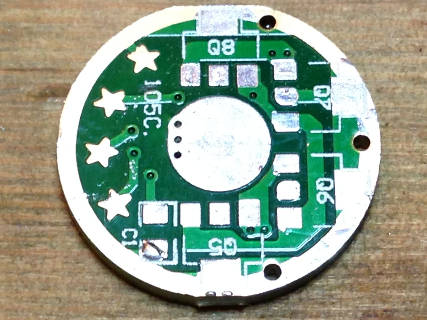
I will be using a 105C board with the 7135’s removed and the mcu replaced with one flashed for me by Dale.
It will have an Lfpak56 FET since I have some(rated for 100A) and fits the board with no overlap of ground ring. The pins don’t match the 70N02 so I won’t be using an Oshpark board.
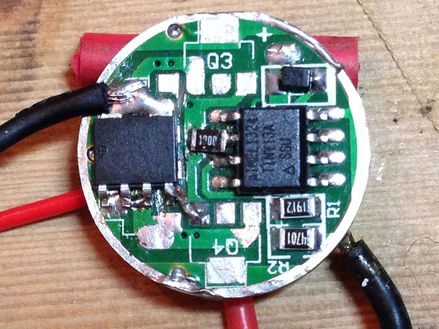
Existing 4.7k R2 and new value for R1(somewhere between 47k and 51k).
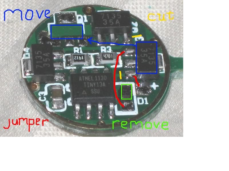
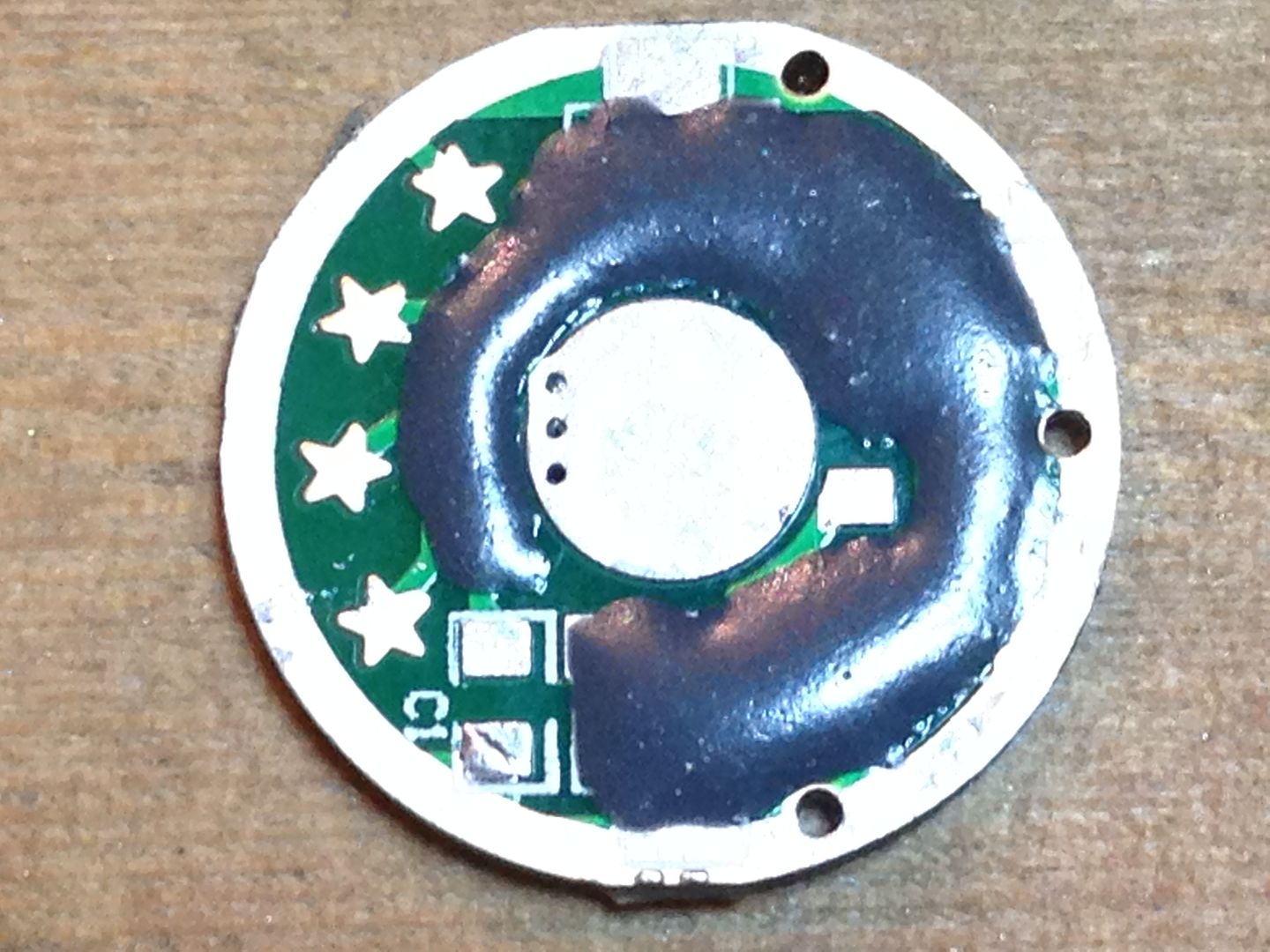
The 7135 position closest too output traces cut, D1 as the jumper for Vin, a jumper wire from Vout to Vcc.
Voltage divider disconnected from Vcc and jumpered to Vin using current L+ pad or somewhere on the pwm trace after D1.
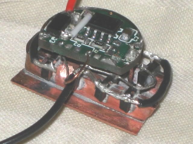
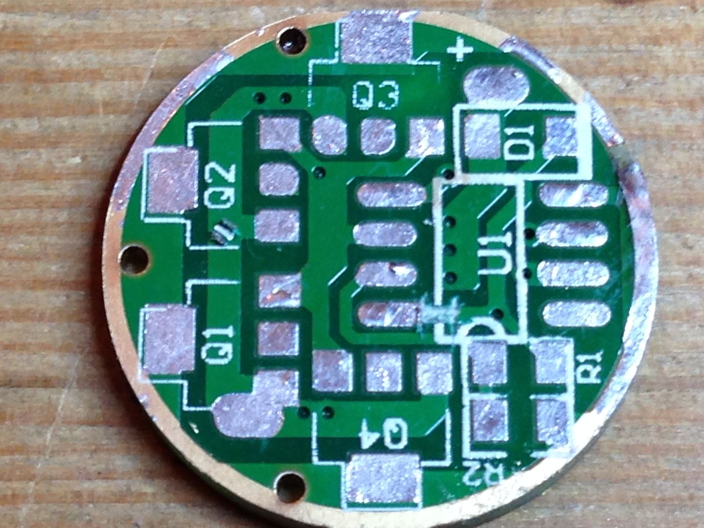
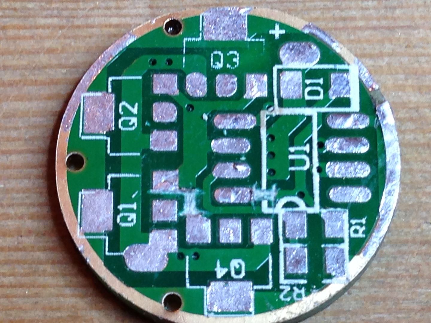
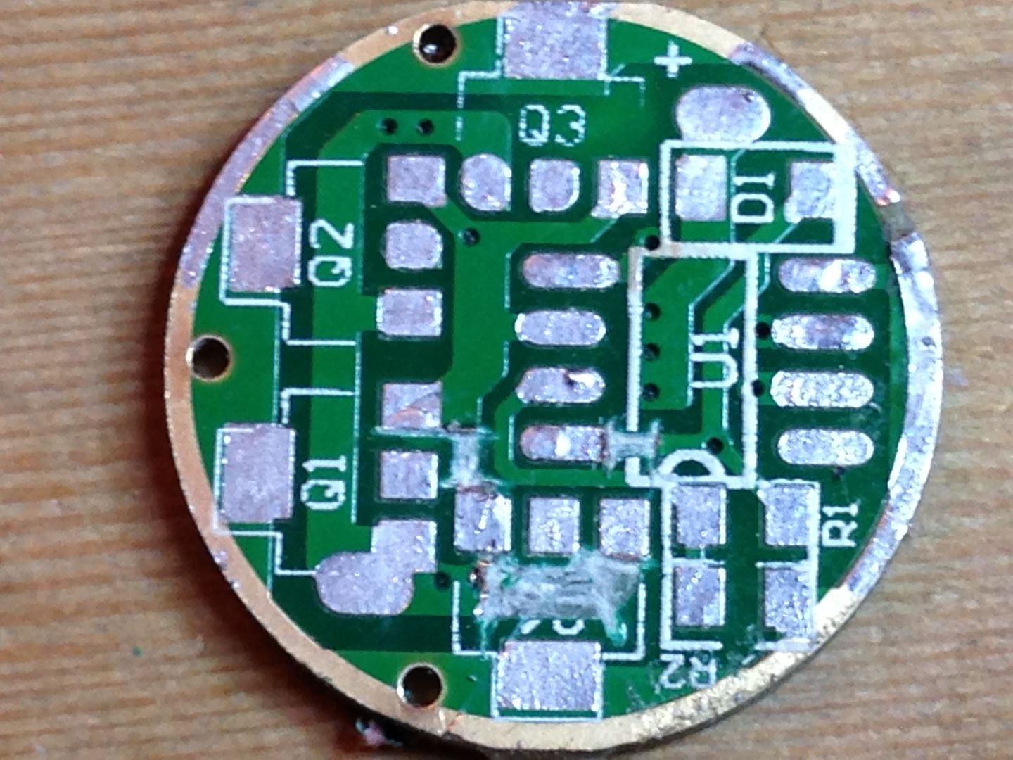
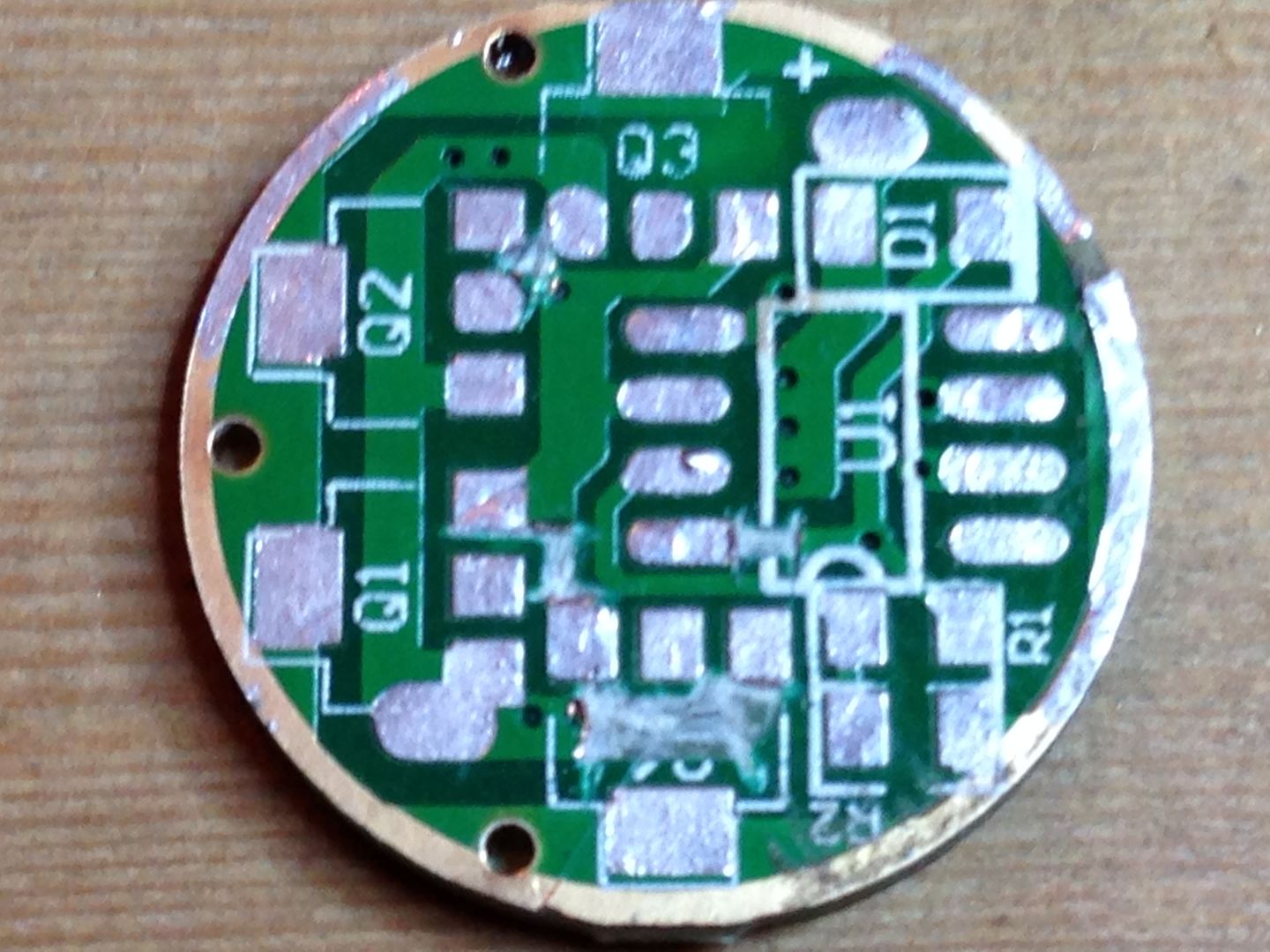
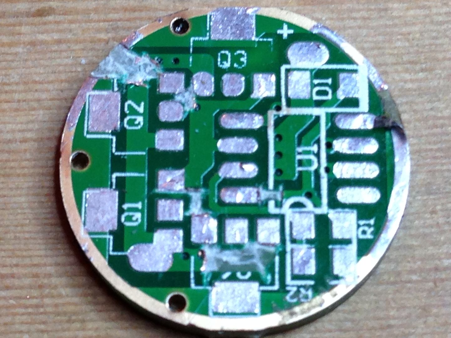
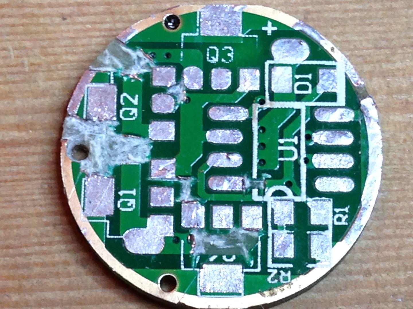
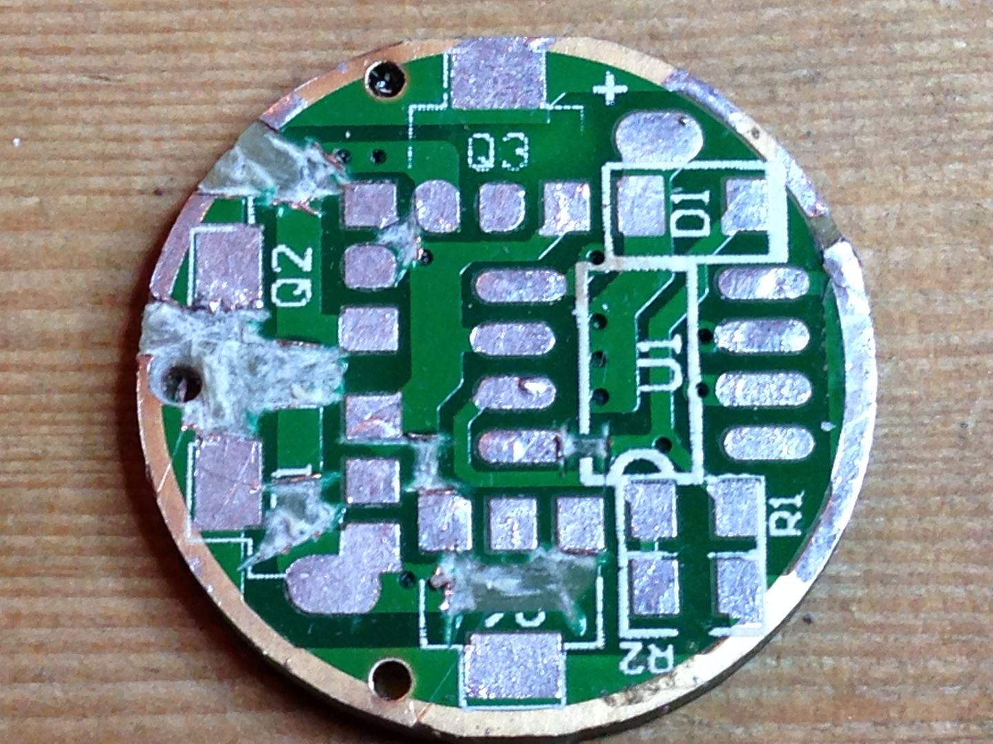
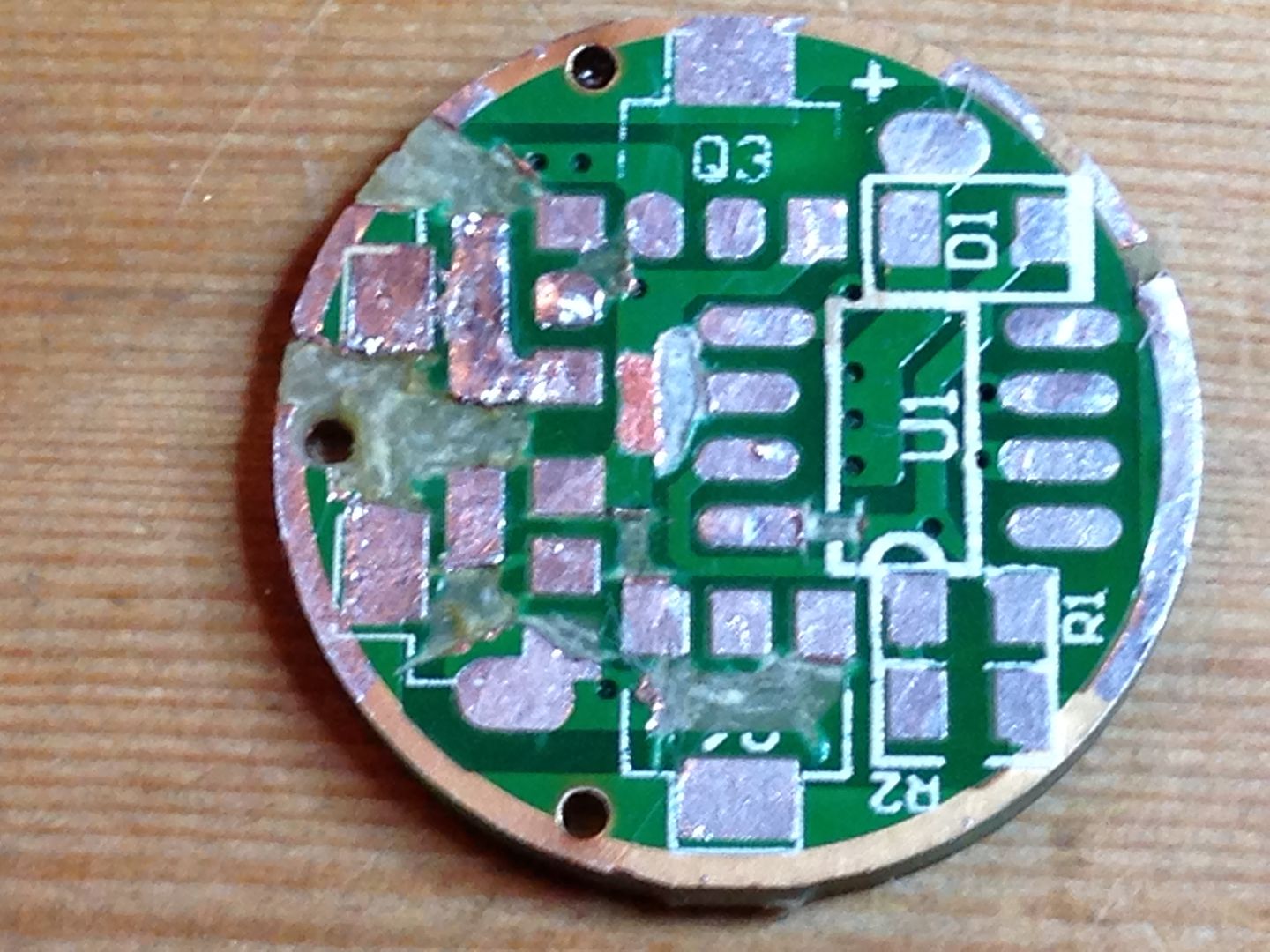
After all the work on the Oshpark boards by others I must be just a glutton for punishment. Here’s a pic of the board I’ll be modifying. Q3 is where I’ll put the voltage regulator and I’m thinking of drilling through the pwm trace for a direct path for L+.
Getting back to the main topic of the thread, if I connect the divider to B+ before the diode I need to know the voltage drop of the diode but if I’m using the same diode and connect the divider after the diode I just use 2.8v per cell to recalculate R1? This doesn’t seem right to me. I think you still need to know the voltage drop across D1 to get the correct value for R1 but wth do I know? Maybe you’re right in that not knowing VD1 won’t give you the exact value of the actual voltage read by pin 7 but will still give you the correct resistance value if you match that offset value. I think I need an Ervin translation. ![]()