I have quite a few custom .lbr
I also use 0603 pads, my 0805 components fit just fine on the pads when I use hot air to reflow the components
Might just give you a bit more space on your placement
I have quite a few custom .lbr
I also use 0603 pads, my 0805 components fit just fine on the pads when I use hot air to reflow the components
Might just give you a bit more space on your placement
Custom Eagle parts makes sense. I’ll have to take a look at these PCBs when they arrive (since I know exactly what Eagle parts I used) and compare with real life 0805 components.
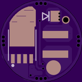
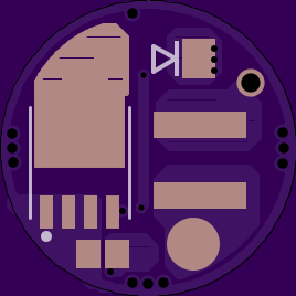
While looking at other drivers I recently realized that there’s no reason for me to fret over the need for a big inductor. I’ve been looking for wrapped toroids like we find on the DRY driver and original SRK driver, but I wasn’t able to figure out where to shop parametrically to find high-current toroids at the desired inductance. Turns out there’s no reason not to plop a (phsyically smaller!) SMD inductor right on top of all the other parts. It’s big enough to easily hookup with an air-wire.
This solves half of the crisis I was running into… the parts on the new-version DRY driver are probably spec’ed for 3-5A, it’s hard to say. zeremefico showed the driver running at 7A, but he did not discuss heat. I assume that at that current the diode and inductor are putting off some heat due to being under-spec’ed. I know people are going to want more current. A bigger diode is possible with a redesign and easy to source. We’ve already got the FET bit mostly figured out, that’s old news. So the missing link was the inductor. ![]()
Big inductors still cost a few bucks and the corners start to poke out past 16mm or so, but I think this is doable.
Just realized that I’ve been developing this driver on a 16mm PCB, not 17mm.
FWIW the lfpak56 is about half the size of the larger fets and is rated for 100A if you find board space tight. There’s an even smaller “33” rated for 60A. The design is only a few years old so it might not go out of production soon like the Vishay did.
Thanks RBD. I’m going to look into that package, space is tight if I try to put an SMD inductor on the board.
The particular DPAK Vishay product we were buying on eBay was no doubt out of production long before we started buying it. Powerful DPAK/TO252 FETs will probably be produced until after we are dead. There should really be no fear of the supply of DPAK FETs drying up.
Well, thanks again RBD. That was a great suggestion, and together with making my work area an actual 17mm circle instead of 16mm (!), that freed up a lot of space. The pin configuration is also different, in a good way. I’ve done a total rework on the board.


So here are the gotchas:
Not a gotcha, but the overall size of v020 is similar to that of a Nanjg 105c - this board is about 1.0-1.5mm taller depending on inductor selection.
On the FET’s that I have the drain is the big tab and bottom plate, the gate is the single pin you have as the gate, and the source(ground) is what you have connected to the diode.
Well that’s bad. Let me go back and look.
I had the part right, it’s as you say. I got those backwards when I hooked it up in the schematic. Grr.
Better now than later. ![]()
Absolutely. It’s actually no big deal, there’s so little going on on the top, and so much space, that it’s just a non issue. I’m wasting a little time making things decent, but I’m not going for really nice at this point. I’ll post a new version in a few.
I am surprised mattaus has not poked his head in yet. ![]()
looks good so far to my untrained eye.
Thanks! Maybe he doesn’t like the cheap, barely documented Chinese IC this thing relies on? ![]()
Here’s the update:


There’s a part connected to pin 7 of the mcu that looks to have both pads connected to ground. Is that correct?
Nope. :bigsmile:
I (almost) wanted to redo those GND vias anyway. They were bothering me.
EDIT: scratch that. I’m totally not “re-doing” the ground vias right now. I did remove the offending vias. As you can probably make out now, that’s the middle of the voltage divider for battery monitoring.

If the space is available, I will spin the QX5241 90 degree clockwise which will shorten the trace.
What parts get hot from losses?
Ideally none ;-). In practice, only parts on top of the board should get hot under any circumstances. I’d expect problems to hit in this order:
Good suggestion. I tried this before, but I was unable to make it work. Since you suggested it, I looked and you are right: that trace seems much too long. So I tried again, this time I made it work.
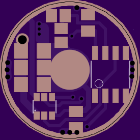
Obviously several traces and vias moved to facilitate the changes. Everything passes DRC (other than all the intentional overlaps & stuff). Minimum trace width on the board is now 13mil (between the ATtiny13A pins), DR allow for a minimum of 6mil.

