- Why? As far as I can see they both fit, it just looks unattractive. This way nobody gets caught with a board/FET pair that don’t work together and has to wait weeks for Oshpark to send a new board.
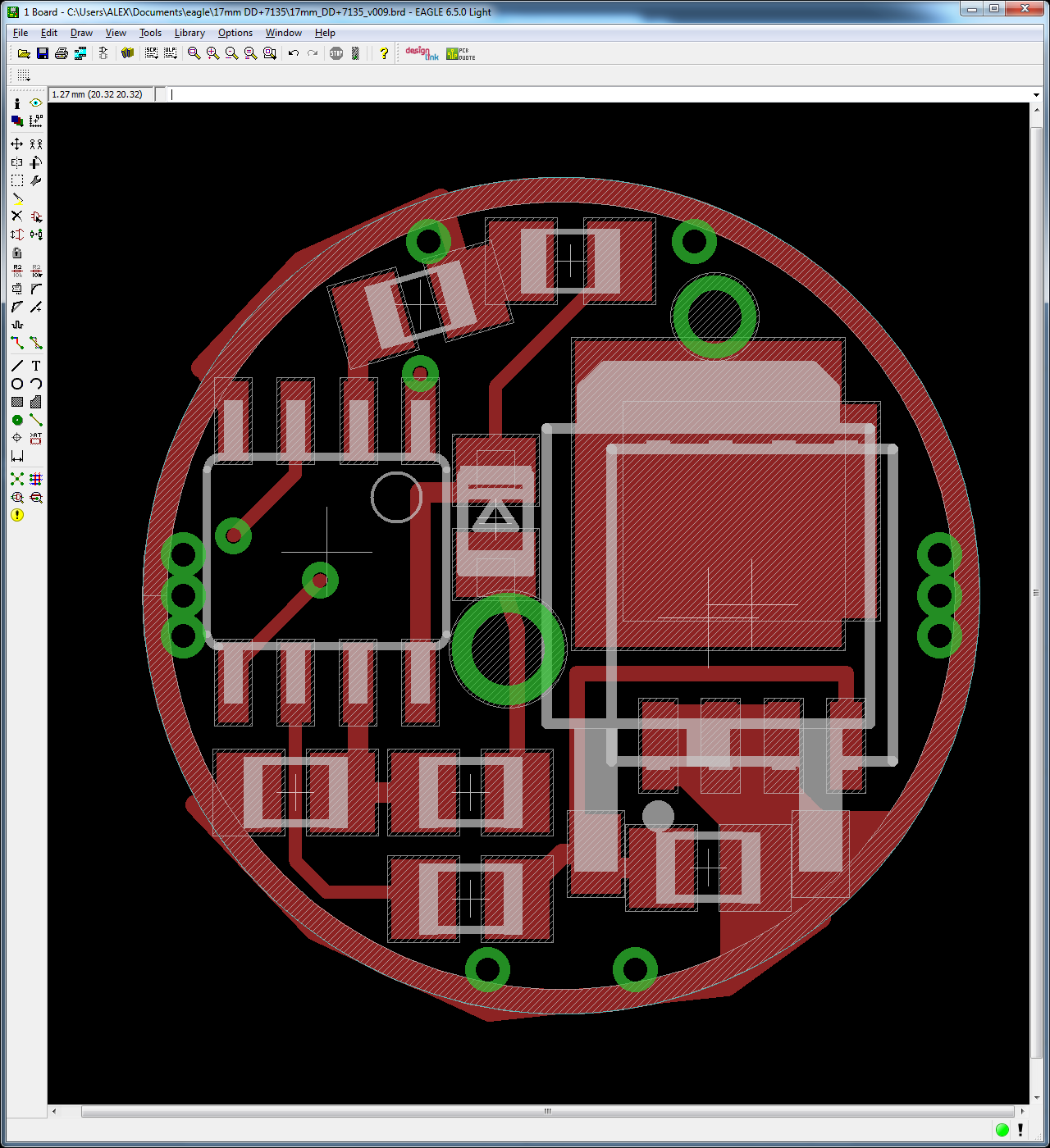
- The pour is 6mm, the exposed contact is 5mm.
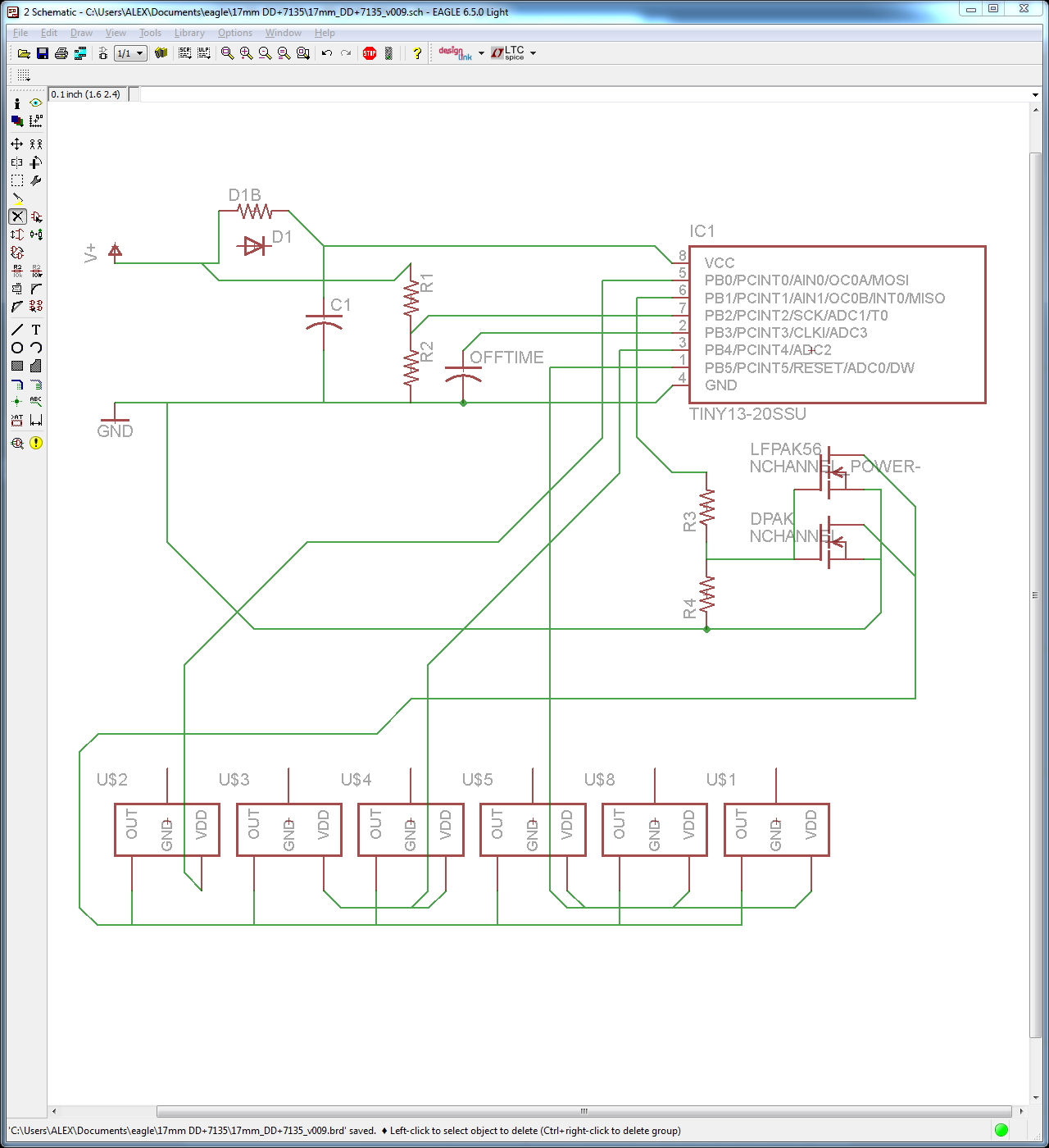
- It uses 4 output pins for that. PB1 is PWM, that is hooked up to the FET. I should swap PB0 and PB4 so that the single 1*7135 is also on a PWM pin (PB0).
- It works the other way too. I figure it’s easier to solder a 0603 on a 0805 pad than the other way around. Soldering 0805 on a 0603 is a minor pain in my butt. Thoughts?
When the time comes I want 8k or more. 8k will hold a bootloader for programming without ICSP. You should be able to program a chip which has a bootloader using 3 wires or less. Header time! Unfortunately the ATtiny85 is probably the best candidate for that and in SOIC it’s only available in 208mil package, not the 150mil we use now. It won’t fit on boards like this one. The MLF package (20M1) is an option, but you can’t bring vias up under it and pass them over to pins like I did on this board. Also realistically it’s reflow only.
Good suggestion. I was being lazy because I do not enjoy working on parts. I should make a new part that eliminates that pin and the stop. That will make it much easier to route in a semi-attractive manner. The trace still may end up under the pin. As long as you don’t have much chance of exposed copper (like a tented via that gets solder down inside it) I think it’s OK to route the trace under there.