No, not really the same I think. You’re looking at a tiny difference in voltage (like 0.1v) vs a big difference in voltage. (like 1.0v)
- I'd remove any extraneous traces from your PCB like the end of the semi-circular VIN ring (top right of underside of the PCB).
- Remove any right angle bends in traces (trace going to gate of Q1).
- Thicken the crap out of the trace from the source of each FET to ground (remember the 'drain' is LED-, the 'source' is GND on an N-Channel FET). They're thick already but they can be thicker...so make them thicker. These are VERY high powered LEDs.
- You're probably going to want to make the LED- solder holes a fair bit bigger as well because you'll need thick gauge wire.
- Ditto for the B+ holes.
- I cannot comment on the technical aspects of capacitor and reverse polarity diode placement, but I can say that from the day I first started designing LED drivers I have always placed my supply capacitor between V+ and GND on the MCU side of the protection diode.
- I have not had a chance to read through and digest comfy's FET/Gate scope thread, but from a safety perspective you should always include an inline and pull-down gate resistor when controlling a FET. The inline resistor will protect your PIC if something goes belly up in the FET, and the pull down resistor prevents the gate from floating; which can also cause problems. If I'm completely wrong on this please don't start a discussion in this thread about it, just tell me I need to read comfy's thread :)
That's all I have for now :)
Design updated while I was commenting. That's what I get for living in the future lol.
- Matt
Ok one more for now, the 8mm ring is not solid copper so its not connected to the GND programming via like it appears, it just displays like it is.


Well that’s kinda what my driver was, 0.1uf and a 10uf across the Bat+, except no protection diode. Had to go to a 1kHz PWM to reconcile the PWM register value to a percentage of max amperage. That could have been an argument for a larger cap than 10uf.
I’ve got the “everything looks good” from tterev3 and went ahead and ordered a set of the 1.1.4 boards below.


kinda got an XMEN look to it ![]()
4 FETs, 4 claws…Sabertooth ![]()
Depeding upon the Vf of the read LED and the battery voltage, you might be able to use two red LEDs in series. That way you get light out instead of burning off the excess voltage as heat.
If the goal is to use Luminus LEDs and do this in a Shadow SL3 then this will not be possible.
Where can one find one of these shadow sl3’s as a host or for under $50? This is a neat little light.
Cereal_killer, you’ve got some silkscreen text over copper. That isn’t going to print and OSH Park warns of unpredictable results. In my experience all they mean is that they can’t tell you exactly how far the fab will “auto clearance” silkscreen near the copper.
Also (I haven’t checked this) don’t forget to make sure that you make the lines thick enough or they’ll be auto-fattened. OSH Park claims that the silkscreen is done by what is effectively a 200DPI printer, so I treat the minimum thickness as 5mil.
Hey guys got some progress made, instead of piggybacking a driver on the stripped factory one which the switch mounts to I’m making a driver specific for this build which the switch mounts directly to for a direct fit, no need to piggyback onto the stripped factory board anymore. (BTW I already have the 17m PIC RGBW driver ordered to play with)


How do I get the “wings” so they’re part of the outline?
I decided to switch to the little baby fet because the AOD3400A Comfy found is capable of 5.7A, I figure 15A+ will be plenty, no need to use the big ones and since I’m using the smaller components (and I dont need the voltage divider circuit either cause the 85-20SU can do it internally) I went ahead and added a white channel to so this driver can fit a wider range of lights.
Do what I do…use the SOT-123 diode instead of the SOT-323, but that is cool driver, oh and de-stop those vias off the attiny Tools>DRC>Masks>Limit (set to something high like 50mm or whatever measurement metric you use) but make sure to go back and stop those VIAs you want to solder to by clicking the via and checking the stop box.
But that is a wicked cool driver man…like how you fanned the small FETs out to the side
To make the wings you will have to draw a milling ARC and attach it to the milling layer, then take the wing from one side, copy, mirror and attach to the other side
I find putting up a grid in view helps make sure I put stuff on the same level thru the driver
wight knows better than me…still an amateur on Eagle
I think you’re going to torch those FETs. Worst case scenario: you learn by doing.
EDIT: WarHawk-AVG, don’t be mistaken. I’m an absolute amateur at Eagle. I only started actually using it after Mattaus posted his Knucklehead V3 and shared the files with me. Before that I’d installed it but never learned how to use it. [I did my battery carriers using an incredibly laborious combination of CorelDraw, Kicad, and PNG importer/resizers.]
That said… yeah, 4 arcs is the best thing I can think of.
Why/how so?
These aren’t current limiting devices. You (and sometimes others here) seem to think of them as regulators. They are absolutely not regulators. If I use a 5.7A max device and pull 10A through it, the device will be “unhappy”.
Current will be based on Vf, total system resistance, and battery voltage sag.
How is what I’m doing not the exact same thing as a single channel BLF driver? I dont understand, why would it “pull 10A threw a 5.7A max device”? Not only would a single battery never support that draw (that would mean it was pulling 30A+ from a battery) but I fail to see how this is any different that the current BLF xxDD FET drivers that we’re all using, both my EDC lights have FET based/attiny drivers… Yes I understand a FET isnt a current regulator, its a relay, the point of this is to be direct drive, these huge emitters can handle it, in my other “puke light” (my RGB TK45) I run a 7135 based driver for real regulation to the little XP-E2’s, the whole point of this driver is to run at direct drive currents but have each channel individually addressable, otherwise I’d just use a single channel 17dd with the emitters in parallel.
v1.3, gate / pull down resistors added (with thin traces in case resistors arnt needed, cut if they are needed)


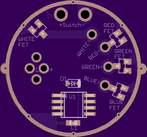
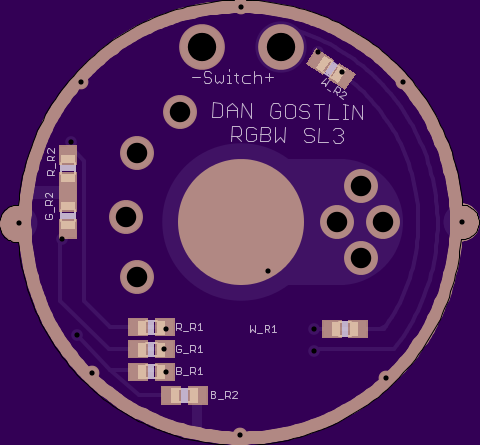
note bottom most resistor should read “BLUE_R2”
new version 1.4 now with wings
This is why:

The current you will pull through the FET is determined by the input voltage, the LED's Vf, and the FET's on-resistance, and has nothing to do with how much current the FET package can withstand before letting the magic smoke out.
I thought the whole point of moving the cap before the diode was to prevent needing the gate resistors (or was that just for ATtiny based drivers)
I was told by comfychair I believe that a FET acts more or like an electronic light switch, a pure wire, on or off, it helped me understand the point of using them…
I discussed that with DrJones since at first I’ll be using a MCU he sends me I decided to go with his way, he didnt specify to use the gate/pull down resistors but did say the cap should go after the diode in VIN (the old way) so i figured I’ll add the pads for the resistors and see if it needed them, if not the trace is there so you dont need a jumper, if it acts strange I can add them in. Plus who knows how it’ll behave without the voltage sense circuit, I decided in the end not to rely on testing on the 17dd and screw myself later having to air wire them in, in general its always a good idea to have the resistors on a MOSFET’s gate so I went with that.
I think you've missed just about every discovery in the 'scope images' thread!
The Nanjg's circuit design with the cap after the diode is inadvertently creating a boost circuit. It runs the MCU right up near its 6v limit in al the PWM'ed modes (effect goes away in the 100% mode), and if (when) there's a tiny spike up above that 6v limit, the MCU shuts down and the light does things it's not supposed to. Moving the cap breaks the inadvertent boost circuit, and the MCU runs at battery voltage minus the voltage drop through the diode, like you would expect it to. This boosting effect happens even on a completely unmodified 8x 7135 Nanjg 105c running any firmware. But adding a FET in place of the 7135s presents a greater load for the MCU's PWM output, and the boosting effect is increased slightly, which is just enough to push things up into the unreliable range. Adding the gate resistor softens the load the MCU has to drive, so the boosting effect is lessened slightly, which has the roundabout effect of lessening the voltage boosting on Vcc. It's a patch, not a cure.
The gate resistor does not-nice things to the waveform sent to the FET gate, it slows down the turn on/turn off times and gives the FET a semi-sine wave signal instead of a sharp clean square wave signal. FETs don't like sine waves, because that leaves them in the bad neither-on-nor-off range for too long. There's a way to stay away from sending the FET a sine wave signal, that is to relocate the cap and get rid of the gate resistor.
DrJones doesn't work with these direct drive FETs, the 7135s will run reliably with the Nanjg's faulty Vcc design without being unreliable. When driving a FET that design no longer works.