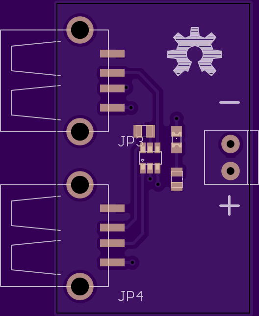
Initially only two sockets worked with “I” devices, I linked the centre pins on the other two sockets, now they will all charge “I” devices. You can see the link on the pic above has just the right side linked.
i was wondering what farty used for the 4 port one…
6 ports and a custom enclosure sounds very cool!
i would like to use one of these with the existing power supply in my desktop, finding someway to thread a cable through the back of the case.
i think it makes a lot of sense, and might save around 10% electricity vs a couple of dedicated ac adapters (my power supply is supposed to be rated 85 plus multiplied by above step down converter at 94, vs 70 found in various adapters…).
I shrank the board, it definitely costs much less (only problem is the daggum silk screen on the top for the USB connectors)
They will have an overhang, a printed housing will be able to fit around the overhang better I believe
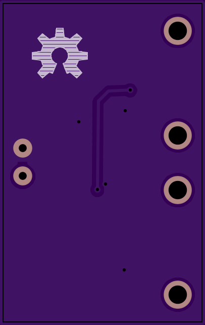
Detected 2 layer board of 2.09x1.58 inches (53x40mm). $16.50 for three.
Top
Bottom
Any input? Is there any way I can hide the silk screen of the USB connectors but not the IC’s (or will it matter on the board size?)
Edit the part. Right click a USB connector > Open package. Change > Layer > tDocu, click each line for the usb outline, save. Back on your board, update the usb connectors. Library > Update all. The usb outline will now be on the tDocu layer vs the chip outlines which will still be tPlace.
Nice thanks…the thing is…the CAM processor I use, the Top Silk layer uses both the tPlace and tDocu layers when it makes the gerber…daggumit
Do you think the above render w/ the tPlace makes the board “appear” bigger to OSHpark thus they charge more, the milling layer is the outline of the bottom image 2.09×1.58 inches (53×40mm) so the board physically will be milled out that size, but I think the silkscreen makes the top image bigger than it needs to be…attempting to fix now
AAAAAND nothing…keep getting an error Library SparkFun-Connectors.lbr was not found in current library path(s). Please adjust the library paths or export the drawing libraries first!
Uggh…went to control panel made sure the SparkFun library is in the directory, I can select them an use…uggh
Good start, but why not switch it up a bit. It should be easy to cut the board down to 1/3 it’s current size and set it up for stacking. You’ve got the ports segregated into two’s anyway. As a matter of fact, I see no interdependence between the pairs anyway! So just make it a 2-port board and be done…. Since you’re mounting them in boxes anyway I see absolutely no reason to make a 6-port board.
If you want to maintain your current port layout (2/2/2/0) you can just make the 2-port version trapezoidal. No reason they can’t fit into the same space. You’ll save money overall (cost per 6 ports will go down) because lots of space is unused in the 6-up version.
I still don’t understand the advantage of putting 3 of these chips on one PCB . The space in the middle of the PCB is wasted… why not just make a PCB with 1 chip and 2 ports and put three of those PCBs in the same project box?