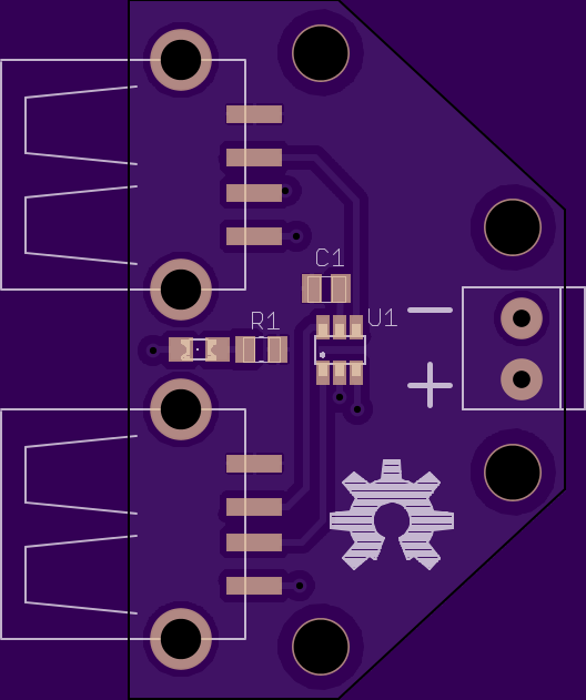
OK…render of the gerbers with updates, I added drills to allow for spacers to stack the boards if wanted (use motherboard standoffs, drill holes directly into the housing of the powersupply, stack 3 boards high, voila), moved the LED between the USB ports to cut down on the glare (we all know those little LED’s can be pretty bright)
This board really isn’t the best, but maybe it will give you some ideas. I noticed that you did not place any components on the bottom, so I didn’t either. My first instinct is definitely to move all the 0805’s and the SOT23-6 onto the bottom. Instead I cleaned up that stray trace so that the bottom is 100% GND. I also connected the shield on the USB ports to GND. I had to move the power LED so I added a second set of pads for that - populate 1 or both sets. Since you seemed hot on the idea of >2 ports, I added a placement for a second set of terminals (for pass through / daisychain). The terminal housings do sit on top of other stuff (SMD pins). Screwholes are M3, so FDD/ODD screws rather than MBD screws. When slimmed down this far the board costs $3.65 for three. I’d say the sweet spot is probably more like $4.50 with a little more space given to everything (mounting considerations, no stacking of headers over SMD pins, etc). Also, I trusted your understanding of the pinout for the chip. I didn’t check the datasheet or anything. Note that I swapped the ports, it was easier to route that way. The corners may be flimsy, but nobody cares if they break off as long as you are using all 3 mounting holes.
I agree. I can’t help wanting to smash the PCB outline as far in as I can get it though ;-).
Even a 2-port stack with all through-hole components and using all Chinese eBay/Aliexpress parts seems like it ends up awfully expensive (and awfully bulky once you strap that ATX PSU onto it).
OTOH you know a good-brand ATX PSU has clean 5v as long as you put a big (wasteful!) load on the 12v to avoid cross-loading (unless it’s a new PSU w/ 5v regulated from 12v… why are you wasting an expensive PSU on charging USB devices though?). And you know what chips you put on the charging PCB. So squeaky clean charging is maybe worth something…
Nice! I put those eurostyle blocks on mine for tying in the powersupply leads, your design could probably benefit from a smaller form factor maybe even header pins
I didn’t realize you were using those terminal blocks when I started (figured it was just a pair of holes ;-)), but really now that I think about it I see no reason not to install them the way I’ve got it laid out. The legs are more than long enough for them to be over top of a little pin or four.
Alternatively you could throw all the low-profile SMD components on the bottom and increase the spacing between the USB ports slightly and increase the length of the board a little maybe. With a single terminal block you could then fit it between the USB ports. You’d also be able to fit 6-32 motherboard screws and standoffs rather than M3 screws.
Actually you might be able to get the overall board size lower that way… hmm…
I’m checking the datasheet and wiring now. (Sunday morning ;)) I think there’s only one error easily fixable for a prototype. You’ve got the decoupling cap inline for the little TP2513’s Vin. That won’t work, the chip won’t get any 5v! (caps block DC…) Take another look at the datasheet. See how the decoupling cap just connects between the Vin trace and GND but Vin also connects to 5v?
Yup…gonna have to do some revision…the cap doesn’t have a passthru to the + plane of the board…doh, can easily scrape the edge of the mask right below the C1 silkscreen to raw copper and solder a jumper
Might even rotate the chip like you did on your board wight…to cut down on the trace length
I am really digging the look of the board with the large polygon pour though, will be fixing…
wight, do you or anyone else know how to remove the white silk screening of the component on the copper pads under the tStop layer? I want it to print the outline of the IC but not print over the copper, I can gently scrape it, but would rather not have to
Um…yes they do (at least they did on this run (was the 5 day expedite test)
It’s a crappy pic…but the white outline and little feet of the 6 pin IC is printed over the top of the pads, heck they even printed the outline of the USB housing over the bare copper of the VIA, everything else is spot on
I even scraped one to ensure…sure enough raw copper under the white paint
wight, I found a better way, bridge the capacitor, solder the cap from the end pad to the ground pin on the USB A pin
I might just trash these and get another set after I do the fixes
There were errors on those boards anyway…my mistake, won’t get them to remake them
Besides I believe I fixed my screwup
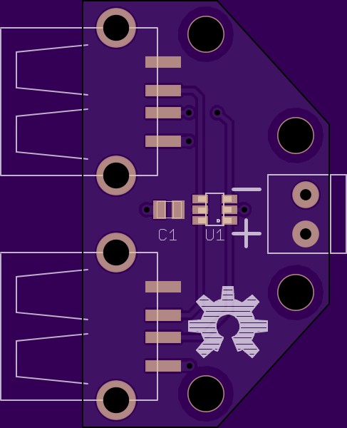
Even shaved a little bit off, and removed the more or less useless LED and resistor
2 layer board of 0.87x1.5 inches (22x38mm). $6.50 for three
Wight, and/or others…wanna check it out please
Render
Top
Bottom
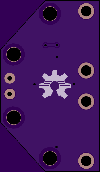
A little 3D
Files
Oh and Halo… I sent them OSHPark an email…this production was under the Super Swift Service “test” they might have skipped that step in the rush…but thanks for the heads up on the producers removing the mask, Thanks!
um…duh…click the thermal outline, properties…actually had to turn off thermals for the pads to be solid instead of the broken pattern
Thanks Halo…
Do you guys want the “status led”?
More or less going to be on all the time the board has 5vdc applied to it
Files updated with thermals off (no render, same as the above, just now instead of having to draw a trace over the thermal cutout area and having to name it, it removes the auto gap created by the thermal parameter)