I was thinking about these, but they are 8mm.
Edit: Head OD looks to be <45mm, so the above wont work.
I was thinking about these, but they are 8mm.
Edit: Head OD looks to be <45mm, so the above wont work.
Ok I’ve been studying the .sch for 2 days now, I was going to ask this in email but I figure I’ll put it here for everyone…
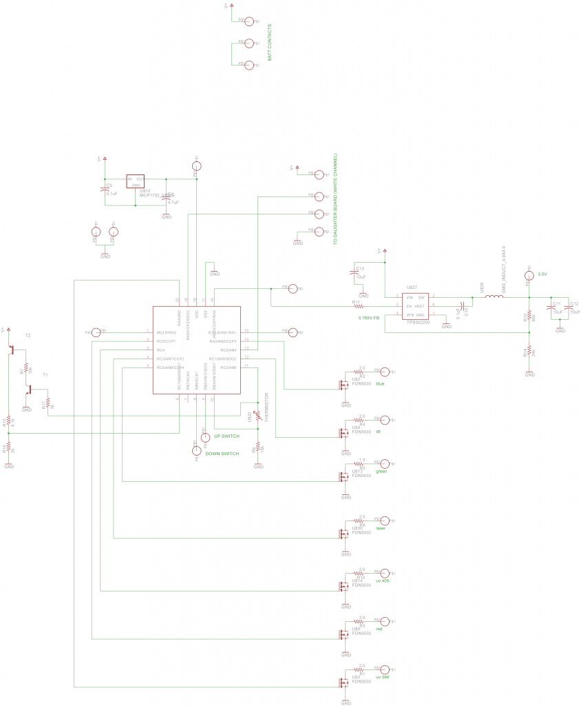
It’s the TPS562200 that does the bucking for the color / UV / IR emitters correct? And it looks like either R12 or R14 is the sense resistor for that (tho the values seem high for a sense resistor). So what if multiple emitters are on at the same time, they would get current split like if they were simply paralleled or the chip will increase current to compensate? What’s the max current?
The other question is about what’s going on with the FET and what I assume to be a BJT up top powering the MAXUM chip, this is obviously to shut it down cause of its standby current, what exactly does this circuit do tho? Specifically what does Q1 do (and R9 is just a gate resistor right)?
Right
these two form a voltage divider which sets the output voltage by making a 3.5v output produce a 0.765v level at the feedback pin, which is the setpoint the chip is regulating to. The chip has no specific output voltage, and in fact it doesn’t know or care what the real output is, it just regulates to 0.765v on the fb pin. The manufacturer does this so that the same chip can be used to produce any voltage you want.
You’re thinking of constant current regulators, but this is constant voltage for exactly this reason. The led currents are individually set by their resistors next to the FETs, so you can have any number on simultaneously and their currents won’t change. The regulator will supply whatever current it needs to in order to maintain 3.5V, so yes it will compensate automatically. The buck regulator is set at 3.5v because from this voltage I can easily set led currents with resistors while minimizing the wasted power because the voltage overhead is low.
It can supply up to 3A total for the color leds
Q1 is necessary to protect the microcontroller from high voltage and to allow the FET to completely shut off. If you connected directly to the FET gate, when you tried to turn it off by setting the uC pin high, the FET would still see (Vin - Vcc) which could be as high as 12.2-3.3= 9.3V, so it wouldn’t turn off. You could then try setting the uC pin to high impedance and let the FET gate pull-up resistor turn it off, but then your uC would see as much as 12.6V on the pin, which would waste current at best and destroy the microcontroller at worst.
R9 limits base current into the BJT. BJTs are current-controlled unlike FETs so you must regulate base current to keep from destroying them
Ok one more Q,
The 3A total to the colors, that’s limited by the TPS regulator or the FET’s?
That’s the regulator’s limit, I set the individual current limiting resistors so that total current draw can’t exceed that. I plan to set most of the colors around 700mA
Ok well looked up the datasheet and turns out I have a few more Q’s still…
It states 2A max, I’m assuming you’ve used this chip before and already know it can do 3A? You must be using the TPS563200?
What’s the reason for having the sets of 2 parallel cap’s (C11/C12 & C13/C14) instead of just one at each location? To keep them from getting saturated? Also I notice you’re using quite a bit less total capacitance on each of the pin’s. I believe I remember you saying this is the exact chip you use on your MELD driver, so I assume your way works fine, why the difference from spec?
Actually you’re right, I had 3A in my head but I’m using the lower power version. The firmware only allows ~1.4A maximum at one time with all colors set at 700mA so it won’t be an issue.
You’re right that the amount is low, I generally just put the 0603 package on there and then fit as much capacitance as I can. I’ll probably get more than 20uF total on the actual board. The reason to have multiple caps is to layer them for better filtering—a 10uF in parallel with a 0.1uF will filter out high frequency crap much better than a single 10.1 cap. The reasons for this get into much more science than we should include here I think…
Here’s the final version of the schematic with a few updates:
So today I’m looking at the voltage regulator for the MCU and I see it’s polarity protected which effectively protects the MCU, are any other components susceptible to batteries being inserted (regardless if any one, two or three are inserted) wrong?
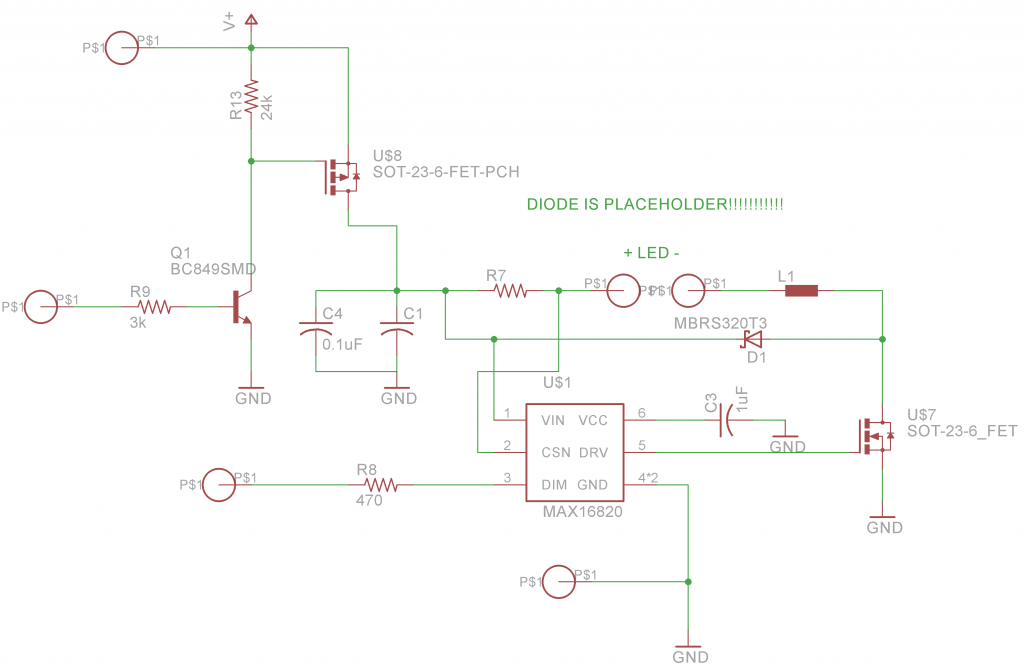
I’m not sure how the TPS562200 or the MAX16820 would handle reverse voltage. Both would be fully exposed to it if the batteries were put in backwards.
Mixing up the directions is another matter—you’d be applying reverse voltage to one of the cells which could get dangerous.
I have polarity markings and springs/contact plates which both differentiate the cell direction, I’m not too worried about them getting mixed up.
Do not underestimate the resourcefulness of idiots! LOL
That was not to rain on you parade or degrade your great work at all. Nor your thinking. But I am reminded every day that common sense is fairly uncommon!
Keep it up. It looks like this will be the do-all end all light. Love to read these threads and all the Q&A/R&D that goes on in them though some of it is lost on me :-D
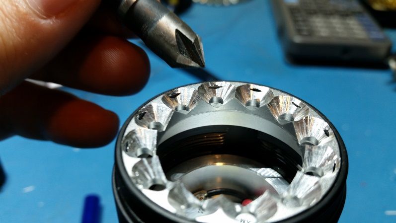
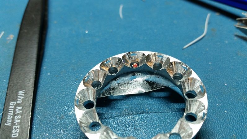
Yesterday I found a countersink bit at the store that looked like it was the right size, so I reamed out the holes in the aluminum ring:
I couldn’t go down far enough to remove the vertical section, but the height should be ok. Here’s how high the XQ sits:
and OSHPark shipped all the boards to me today!
IT WORKS! I’ll get the pictures up tonight
NICE! Looking forward to them :-D ( <- add Drool)
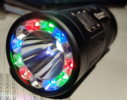
Sneak preview:
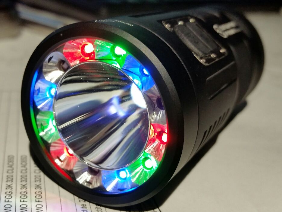
^ That is a thing of beauty. Congrats tterev3 :)
Wow nice!
looks great!
Well done. I love the words it works. Better than cursing.
I was so excited about this project that the timeline looked like this: opened OSHPark packages 5pm Wednesday, LED board and main board populated by 8pm, woke up at 5am to build daughter board and assemble, light finished by 7:45am when I had to leave for work. Yes I’m insane
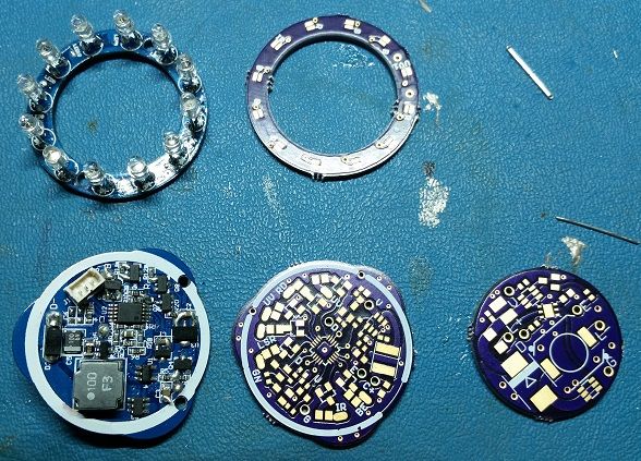
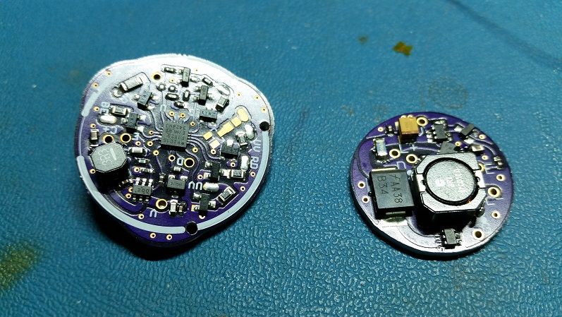
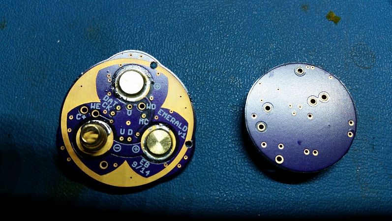
The build went very smoothly. Here are all my bare boards compared to the stock boards:
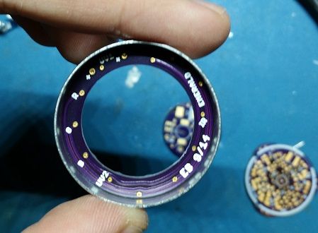
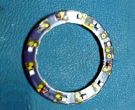
My measurements were good and the LED board fit right into the ring:
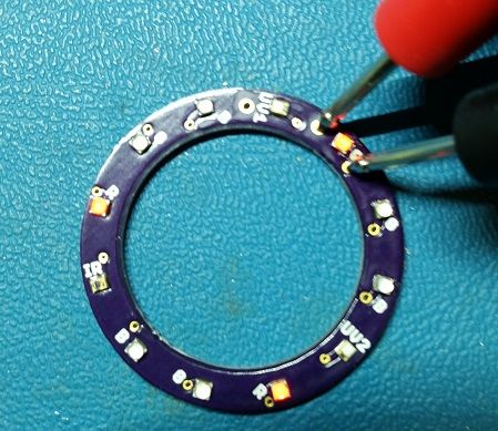
I populated the LED board first. Here’s a shot of the reds under test:
Checking the fit of the LEDs in the “reflectors” formed by drilling out the holes with a countersink bit:
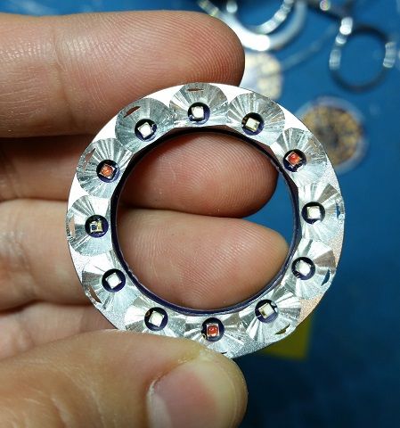
To prevent any shorts against the aluminum, I put kapton over all exposed holes on the top of the LED board:
And then very carefully epoxied it to the ring with arctic silver. It gets pretty good thermal contact since the entire top surface is a fill plane connected to the anode of all the LEDs, and then that top surface is thermal epoxied to the aluminum ring.
On to the real boards. The only parts I transplanted from the stock boards were the battery contacts:
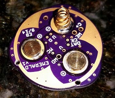
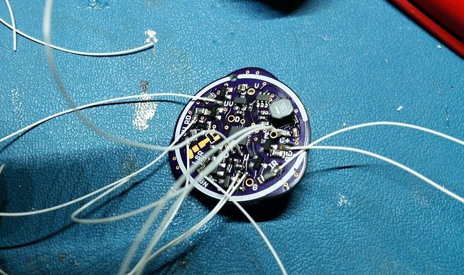
Here are my two boards front and back after assembly:
Before mating the two I added all the wires in for everything that connects straight to the main board:
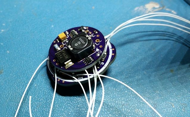
And then I attached the daugher board via its four interconnects (Vin, Gnd, Dim, Enable):
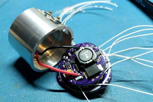
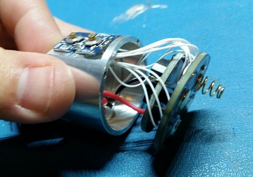
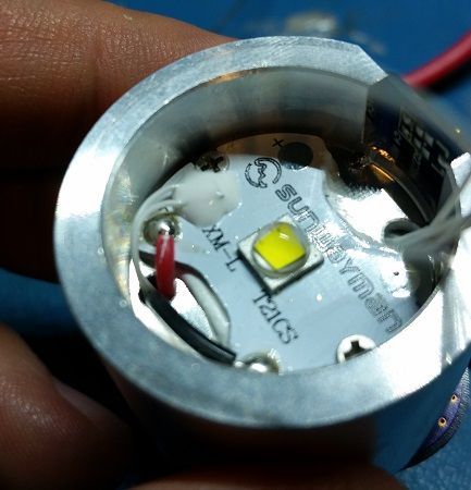
I preserved the original wires, LED, and star board from the stock light, and connected it up to my white channel buck driver on the daughter board:
I kept the original switch board and wired it in, and started feeding all my wires up to the LED area:
The thermistor I used for temperature monitoring is an 0603; I tweaked the wires until it sat down on the LED star:
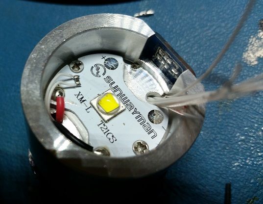
And then tacked it down with arctic alumina:
Then came the fun step of connecting all the wires up to the LED ring:
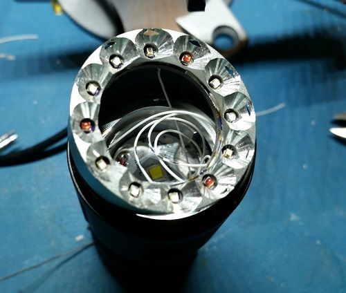
And done!
I’ll do a writeup of the software updates soon. Suffice to say the up/down button configuration makes the user interface so much better
I wondered what you were doing online at 5am lol, saw your name listed before I went to bed.
So do you have other plans for the driver, or more work on this? Noticed it in the sch- the unpopulated pads…