Thanks for the answer about the problems that come with using a potmeter for setting the sense resistor value.
I tried to read through the lambdalight thread with my limited grasp of electronics, but what spoils for me the use of a pot for varying brightness in that type of driver is that the pot setting is converted into pwm after all.
You’re welcome. If you want a PWM free output you can probably implement that by feeding the ATtiny’s PWM into an LD-29. IIRC that outputs a smooth constant current at every drive level, but the MCU outputs PWM.
I agree. I’m speculating that the short “full off” is where we get the resonance/buzzing from, but I could be wrong.
The Rds(on) of SiR800DP is much lower than DTU30N02 while Qg is higher. Another MOSFET I recently looked at is the Vishay SiS414DN. That one has a slightly lower Rds(on) than DTU30N02 while having a lower Qg. The “Output Characteristics” graph looks very similar, while Transfer Characteristics are shifted to slightly lower voltage.
Based on what little I know, I think both are strong candidates for this application. I’ve got to figure out my inventory on other parts and then I’ll place a Mouser order. If anyone has thoughts on other FETs which they feel may be good candidates, now would be the time to speak up.
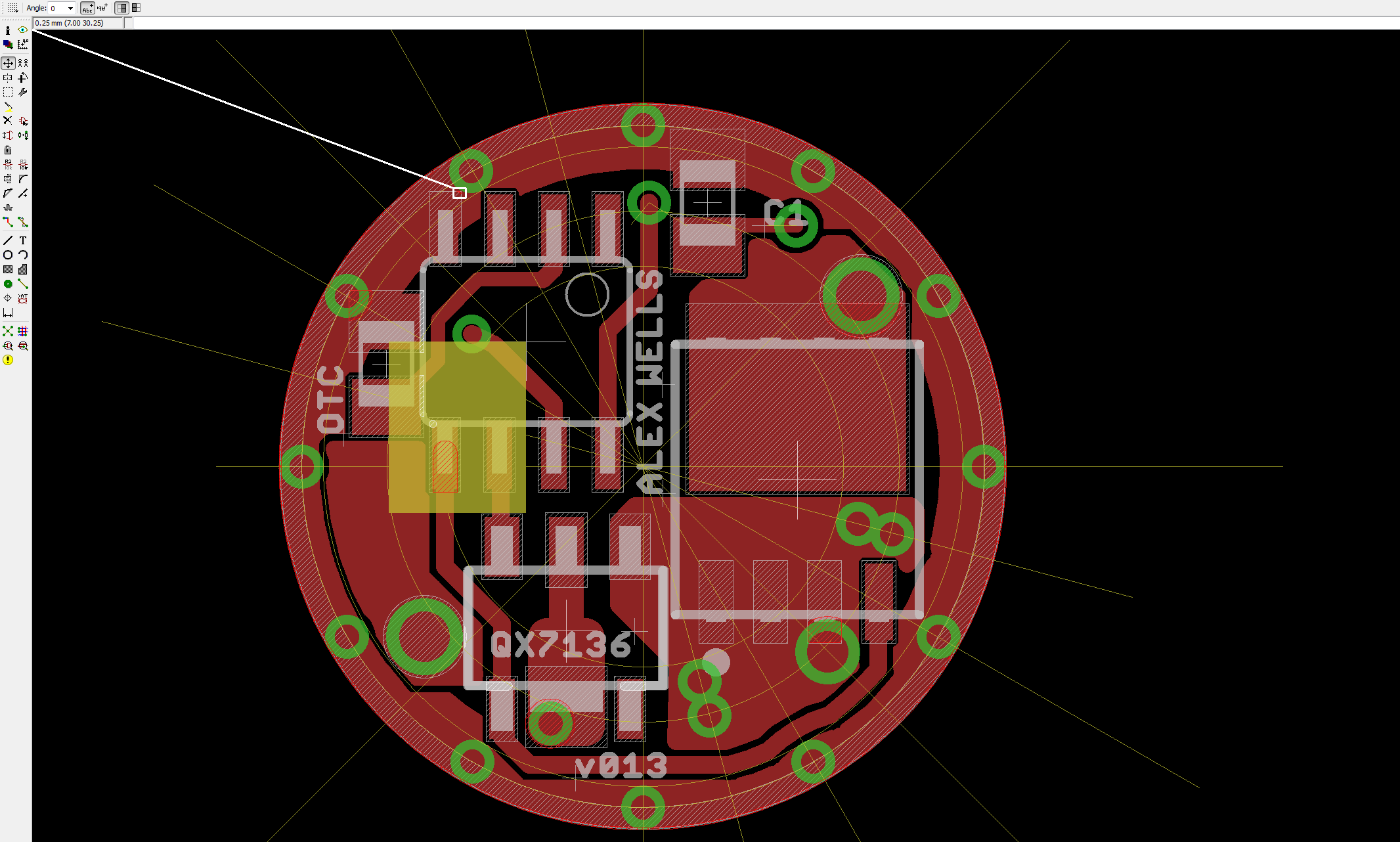
The silkscreen has not been updated significantly, it is messy and incorrect.
The thin horizontal lines displayed inside the larger copper pours are all OSH Park rendering artifacts. The copper pours are solid.
The top PCB is symmetrical, it may be placed face up or face down. It may be “remote” mounted but it must be isolated from the flashlight body in any case of course.
The top PCB is 15mm in diameter and 10mm wide.
The top PCB is designed to be rotated either 55º or 75º. 55º is the recommended rotation and is the one displayed here.
Four (4) size 1206 sense resistor pads are available.
3 connections are required between the two PCBs: GND, Csense, and DRV. Csense is the center connection, DRV is available on the two small vias, and GND is availble at the end beyond the sense resistors.
Two 1.2mm vias are provided for GND on the daughter PCB. The second 1.2mm via may be used to attach GND to a GND screw on the pill.
LED+ connects to the bottom, parent, PCB and bypasses the daughter PCB. LED- connects to one of the four 1.2mm vias next to the FET on the daughter PCB.
(This board is not available to order since I just slapped two boards into one Gerber.)
Using my low-end test equipment with the driver regulating at 2.45A and no reverse polarity protection diode dropout appears to be ~0.24v. Not bad, but I can certainly imagine better.
I’ve just measured a single 7135 regulating at 0.37A, no reverse polarity protection, and dropout appears to be ~0.18v.
Hey Alex, any updates on this project? I have always been fond of the Supfire M6 driver that uses the 7136s to drive each of the three channels. As we talked about earlier, however, they implemented some sort of strange network that the PWM signal passes through before going to the 7136s. I haven't had time to investigate further, but it seems bizarre that they would add all of those components for no reason. Although we have seen those guys sometimes put components on boards for no good reason at all, I think it's worth investigating further.
RMM, I’m ordering parts tonight. I’ve been putting it off in anticipation of finding more parts to pile into the same order, I’m terrible about that…. I think I’ll have some test PCBs in hand any day now.
I did scope the test circuit and it seemed to operate fine (Post #18). Until you brought up the extra stuff again just now I hadn’t thought any more about it. I suppose that we could cram in those extra components, but right now I don’t see why. When I have a test platform I like better (an actual assembled driver) I’ll scope that again and then compare that with the M6 driver on the scope. If I had a theory as to what the purpose of that stuff was I’ve forgotten it.
Ugh, what a hobby! Mouser just cleaned out my pockets again. I’ve got several MOSFET candidates in route as well as a small assortment of high-wattage low-value 1206 sense resistors and a couple of 0.02-ohm 0805 sense resistors. I plan to switch these things to 0805s in order to make tuning easier. The overall build cost does go up a little, but I think it’s worthwhile.
… and a new Pomona 5250 clip because I’ve been hobbling along with a damaged one for some time now. I hated to bite the bullet on that since the damage was 100% self-inflected (I shouldn’t have ever put any force on that little pin and I knew it.) It’s dumb to punish myself over a $13 part though, so in the cart it goes.
It’s been a little while since I worked on this driver and I was confused about the purpose behind this large via:
At first I thought it was for wiring since it was 1.2mm. v010 is the last version I when I worked on the driver previously and you can see that the vias in this area were playing havic with the routing of that gate trace. Eventually I realized that the via was for carrying power and that there was no way you’d ever want a wire in that hole.
Moving on, below are a couple of images of the current state of the 17mm driver. In each picture you can see a single DRC error highlighted in white as an example. When I say that a design passes DRC, I am not being literal. All of my drivers fail DRC with amny errors. Generally that’s either because of me ignoring best practices in some way or not setting up my DRC properly. The examples show a GND pin being too close to a GND via in the top (red) image and a pair of the extra-large solder pads I use for 0805 components [the stock Eagle part] overlapping on the bottom of the board. When I say a design “passes DRC and is ready to go” or similar, I’m probably only referring to the portions of DRC which pertain to the fab successfully producing the board.
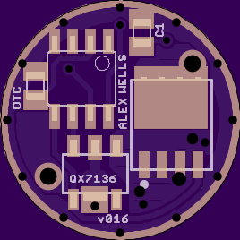
After a little more tuning, here’s what we’ve got. I didn’t mean to leave BLF and the identifiers at the top upside down, I’ll correct that in the future.
As you can see I’ve:
Refreshed the via ring to be more attractive. Previously I rotated it slightly (on purpose) in order to help maintain separation on some things.
Moved the OTC, turns out I was doing an unnecessary component keepout on the ends of the ATtiny13A. The clip clears the area I’ve put the OTC into just fine and this position helps with the new via ring.
Switched to 0805 sense resistors. If you want to usea pair of 1206 there is enough space, but it may require some very minor surgery.
Added/extended large pads on both LED+ and LED- in addition to the large 1.2mm vias.
Vias and traces moved around and cleaned up.
Come to think of it, the purpose of that cleanup was to allow me to double the density of the vias (12 -> 24) of the vias in the GND ring. I need to go back and do that.
This still maintains the strict keepouts around the edge:
1mm component keepout. No physical objects w/in 1mm of the edge.
1mm bare-copper-which-is-not GND keepout. Only GND and covered traces are allowed w/in 1mm of the edge. No vias from a net other than GND and no bare copper from a net other than GND.
I’m thinking that the name needs to not be A17LDQX where the LD stands for linear driver and the QX stands for QX Micro Devices (QXMD, the IC manufacturer). Initially I thought that the QX7136 was unique to QXMD, but it turns out that 7136’s are also made by others such as MicrOne, whose products we’ve become familiar with around here in recent years. Here’s their MEL7136.
For now I’ve just changed the name to A17LDX where the suffix represents linear driver and an “x” for xtra powerful or xtreme or whatever thing the X normally represents in these situations.
Looking good! I see that you're going back to the LFPAK FET?
I might be losing my mind but I am pretty sure that early on I swapped out one or all of the 30N02 FETs on an M6 driver with 70N02s and it worked. Another trial with an M6 driver may be in order.
I did some more work with the scope tonight. The pictures in post #18 are all of what’s happening on the gate. What’s not visible in those gate shots is that in some modes with a DTU30N02 this does result in the LED being turned off extremely briefly.
Of course in 255/255 we get smooth output at a constant current.
From 254/255 down to at at least 220/255 (but probably lower) we do get the sharp, brief, off as part of the waveform. Modes are producing a fraction of whatever the set current is. Bypassing the sense resistors like RMM does in his Mod Option 2 for the Supfire M6 will certainly affect all modes in that range. (I assume that it will cause the driver to behave like a DD driver, with those modes being fractions of DD current.)
At the bottom of the range we don’t see the sharp dip start to appear until maybe 45/255. In the 0/255 through 45/255 range bypassing the sense resistors appears to make no difference. If anything affects output it may be Vcc/Vdd on the QX7136 IC. I did not experiment with varying that.
Interesting stuff. Really this kind of quirk is more in line with what we might expect for an inexpensive linear CC controller when it’s being semi-abused like this. Nothing’s changed of course: I still expect that the actual performance should be just like one channel of an M6 driver. My shipment of LFPAK56 FETs should come in tomorrow (although I may not be able to do any testing tomorrow.)
SiR800DP behaves just like SMN3R0-30YLD and Vishay 70N02. Totally unworkable for dimming. Full blown 1-mode works fine. (1 regulated mode + unregulated turbo should also be fine although I did not test.)
SiS414DN - I forgot that this is an entirely different footprint. No wonder the “package limited” values are lower than LFPAK56, it’s not LFPAK56! It’s actually PowerPAK1212-8, a much smaller package. I may attempt to test with it, but it will not be convenient to test without new PCBs.