Are you referring to the original, or the latest? This is exactly why I didn’t want Mattaus to reset the version numbering in the way he did. You say “original” but in the same breath say “v1.0” which is the designation for the latest version which Mattaus has released.
I can build the original and compare it to the A17DD-S08 if that would be more prudent than the Ver 3.1?
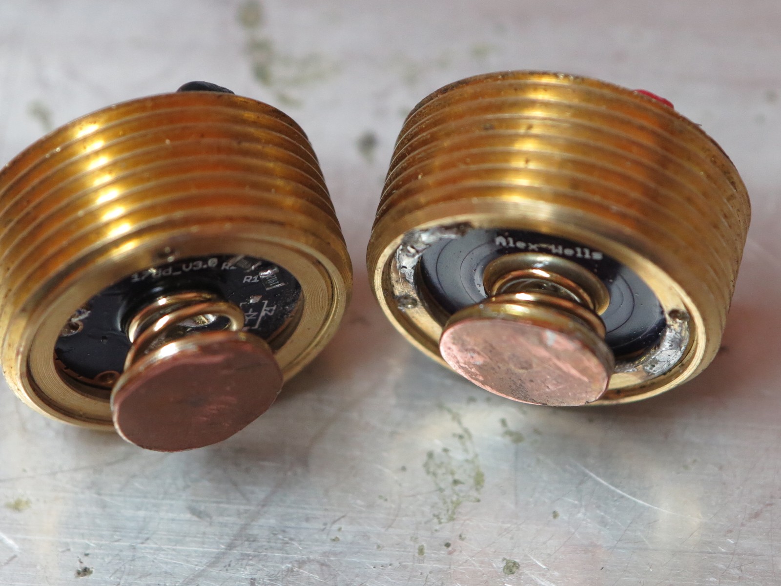
By original , I mean the one with no ground contacts on the spring side, the original , aka, first board.
I don’t really have an opinion on that.
Ok, I’m about to build 2 lights…one with an A17DD-S08 and the other with a BLF17DD Ver 3.1. I will use AVRGCC44 with the A17DD-S08 for the 22,000 R1 to work at 3.0V and 2.8V and the AVRGCC45 with the BLF17DD Ver 3.1 for the 19,100 R1 to work at 3.0V and 2.8V. All other settings are the same.
This has 7 mode levels at 0, 3, 9, 27, 73, 140, and 255.
I’ll be back!
What is a BLF17DD v3.1? Am I missing something here?
The way to go is to use different drivers in the same light, with the same emitter and the same LED wires. That way there is only 1 variable changed. Using different emitters is a bad idea when you're trying to test for 0.2A difference.
Done! I have 2 identical M1’s but different driver styles. Before assembling the emitter/star into the pill (I reflowed them both) I checked Vf on a Sanyo FJ and each had 3.61Vf at 5 seconds on direct drive. These are XM-L2 U3 1A on the new 20mm Noctigon that has temperature sensor pads and the contact pads are closer to the edge (wider stance)
Both have the large bronze phosphor spring from Intl-Outdoor, upside down, and a copper disc soldered to the wide end for ease of use with various cells (flat tops or button tops) No spring bypass due to the spring type and no spring bypass in the tail cap of either light.
So, what kind of tests do we want? Vf on the same cell fresh off the charger each time?
Amperage on the same cell, freshly charged each time?
Amperage in the lower modes simultaneous to the Turbo reading? Or separate from that reading?
Lumens in each level, again on the same cell and freshly charged for each light?
What am I missing?
The BLF17DD Ver 3.1 is the last variation on the 70N03 FET driver, rearranged by Cereal_Killer for an easy Zener modification with Zener pads on the board. The difference between 3.1 and 3.0 is that the Voltage Monitor set-up is taking it’s reading straight off the batt + pad for the spring, before the diode and or Zener. Dan didn’t change the silk screening so it still reads Ver 3.0, but the trace can be seen coming off the resistor bank for the Voltage Monitor.
I am not organized enough, engineer enough, patient enough or willing enough to use the same emitter on different drivers and do all that testing. I have 2 emitters out of the same tape, side by side, that both test at the same Vf on the same cell. That will have to do or I’m done here and will just use the 2 lights and call it even.


So I have 2 Convoy M1’s that make just under 5 lumens in moon, 1405/1455 in Turbo. Worth the doing at any rate. 4.59A from one, 4.50A from the other. Head to head each holds it’s own.
Looking good. 0.09A is nothing. All of the lights I've built with the small LFPAK have all seen very similar performance to what I usually get out of the big FETs.
While the A17DD-S08 did indeed pull .09A less than the BLF17DD Ver 3.1, the A17DD-S08 is the one that logged 1455.9 lumens! ![]()
Not enough difference to be statistically significant.
OT: how do you like the through hole wire vias on the 3.1 driver? I personally would rather have a flat pad to solder to, but I'm wondering what everyone else's opinion is.
The through hole via’s are nice at 22ga, a PITA at 20ga. Forget about 18ga. (Actually, I’ve split the end of 18ga and run each half through a via, works ok, still a PITA. Not pulling any pads off though.)
I like the extra ground via beside the FET ground leg on the A17 board and the big pad is good for soldering the LED - lead to. The middle of the board positive LED lead is a bit on the tricky side though. Not horribly bad but fairly easy to mess up if you jitter instead of jigger. Shimmy instead of shake? You know what I mean….
The microscopic switch+ via on the Ver 3.0/3.1 board is nuts! And the location is tricky as well.
Single sided makes up for a lot of things though, love that aspect! Really makes it easy in a lot of lights, piggybacking too.
Edit: Point being on the comparison…the smaller FET meets or exceeds the performance level of the large 70N03. ![]()
Nice job Dale.
I used a new Panasonic NCR18650BD button top and charged it again after every test. So each “run” started with the cell showing 4.21/4.22V (it must have been like 4.218 or something because my meter, 2 decimal point digits, flickered back and forth between 4.21 and 4.22)
………A17DD-S08……………BLF17DD Ver 3.1
0.01A ——–4.52 lumens……0.01A——–4.55 lumens
0.06A ——22.94 lumens……0.07A——23.08 lumens
0.13A ——51.13 lumens……0.11A——50.34 lumens
0.35A —–148.70 lumens….0.31A—–140.42 lumens
1.15A —–421.59 lumens….1.12A—–400.89 lumens
2.28A —–807.30 lumens….2.36A—–772.80 lumens
4.50A —1455.90 lumens…4.59A—1404.15 lumens
One would think I used 2 of the same everything, they’re so close. I think the A17DD-S08 is doing a fabulous job, and in my triple and quad lights it’s definitely up to the task. ![]()
Thanks again Wight! ![]()
Edit: Notice the low high end amperage, and the resulting lumens output. The new XM-L2 U3 1A’s…
Dale,I think it's simpler to just measure parasitic resistance of each driver.And based on that number you can tell which driver will provide more current on high(if all other factors like battery,led Vf,springs wires are the same).
For DD drivers this is very easy:you need one ammeter and one relatively precise voltmeter,battery or power supply(better),led or resistor as load(not important,xm-l,xp-g...).
Connect driver,led and battery(or power supply) as usual(you don't need host),and ammeter in series for current measurement. At the same time measure voltage(mV range) across driver's "power" connections-GND and led cathode pad.
Parasitic resistance is then: R(par)=U/I
And that's it,repeat the same procedure for other driver(important thing is that it's best to use the same battery at same voltage and same load,because mosfet parasitic resistance Rds, which is dominant part of total parasitic resistance in DD drivers, depends on gate voltage).
You’re saying if I measure the off amperage at the negative end of the cell, and the Voltage between LED negative and ground, then divide which by which to get parasitic resistance?
Touching the LED negative to ground will normally give direct drive, right? So this is where I take a Voltage reading? While taking an amperage reading at the tail?
I’ll either pull the light engine and do this, or remove the bezel and use the host as a holder for the assembly of light engine/cell. I can use my older DMM with short 12ga copper leads to do the amperage reading, my clamp meter with probes hooked up gives very small Voltage readings.
Edit: Is the lower parasitic resistance driver the one that will make the highest power output?
Yes, lowest resistance will give the highest output.
On the A17DD-S08 I get a current of .01 and Voltage of 1.867
On the BLF17DD Ver 3.1 I get a current of .06 and a Voltage of 1.885 ( I think this one skipped moon and the test was on level 2, is that crucial?)
Edit: Was I supposed to be testing on High or does it matter? These numbers come out significantly different…
Ideally you would want to test them both on the highest level, so PWM response isn't a factor.
Back to the drawing board ![]()
See? If it can be done wrong, I’ll find the way…
Edit: It’s better to grow a few new hands than to enlist my wife for help.
A17DD-S08 shows 4.82A and 30.0mV
BLF17DD Ver 3.1 shows 4.85A and 103.5mV
EditII: So is this A= .16 parasitic drain and B= .05 parasitic drain?