A17LDGTO
I did some more work with the scope tonight. The pictures in post #18 are all of what’s happening on the gate. What’s not visible in those gate shots is that in some modes with a DTU30N02 this does result in the LED being turned off extremely briefly.
- Of course in 255/255 we get smooth output at a constant current.
- From 254/255 down to at at least 220/255 (but probably lower) we do get the sharp, brief, off as part of the waveform. Modes are producing a fraction of whatever the set current is. Bypassing the sense resistors like RMM does in his Mod Option 2 for the Supfire M6 will certainly affect all modes in that range. (I assume that it will cause the driver to behave like a DD driver, with those modes being fractions of DD current.)
- At the bottom of the range we don’t see the sharp dip start to appear until maybe 45/255. In the 0/255 through 45/255 range bypassing the sense resistors appears to make no difference. If anything affects output it may be Vcc/Vdd on the QX7136 IC. I did not experiment with varying that.
Interesting stuff. Really this kind of quirk is more in line with what we might expect for an inexpensive linear CC controller when it’s being semi-abused like this. Nothing’s changed of course: I still expect that the actual performance should be just like one channel of an M6 driver. My shipment of LFPAK56 FETs should come in tomorrow (although I may not be able to do any testing tomorrow.)
- SiR800DP behaves just like SMN3R0-30YLD and Vishay 70N02. Totally unworkable for dimming. Full blown 1-mode works fine. (1 regulated mode + unregulated turbo should also be fine although I did not test.)
- SiS414DN - I forgot that this is an entirely different footprint. No wonder the “package limited” values are lower than LFPAK56, it’s not LFPAK56! It’s actually PowerPAK1212-8, a much smaller package. I may attempt to test with it, but it will not be convenient to test without new PCBs.
- I haven’t tested any other FETs yet.
Foo! ![]()
I'm going to be building some M6s this week and I'll try and swap a 70N02 and a few different ones in there to see if they work in that setup.
Thanks RMM. That would be very valuable!
I’ve been doing some thinking about why SiR800DP did not work. (Again, all the FETs I tried work fine in 255/255 mode. Current is regulated properly, the LED lights up, all good. It’s all lower modes where they struggle.)
If you take a look at the datasheets, nothing is spec’ed as having a markedly lower Qg than DTU30N02. It’s also possible that DTU30N02 comes in slightly below spec and the others are coming in slightly higher. At a glance it appears that “turn on delay time” is also either higher or spec’ed similarly on these other FETs I’ve tried.
What I’m hoping is that reducing PWM freq may fix something. That would be sweet…
Wight, I've only ever done phase correct 9.4 kHz into the 7136s. I wonder if there's something to that? I've never heard any noise at all come from the lights so there is nothing lost by switching to it.
#$@&%* YES!
I was less than thrilled when this thing didn’t work the way I expected with NXP PSMN3R0-30YLD or Vishay 70N02. My scant notes showed that I’d already switched to 9.4khz phase correct, so I dropped in a :8 prescaler to take things down to 1175hz. Since I had a Vishay 70N02 laying there on the bench, that’s what I tested with. It appears to be functioning fine. I haven’t scoped it yet, so no telling what the slow PWM is doing to my output waveform. Haven’t even measured current yet…
- I scoped the output on the 70N02. Looks fine to me.
- I installed NXP PSMN3R0-30YLD. No problem.
Right on! The poor little 7136 must not be able to count fast enough to keep up with the faster input PWM. 
I’m quite excited about this little driver, glad to hear it’s making progress again. I’m getting tired of stacking 7135s and dealing with their tricky heatsinking requirements.
Something like this would be a perfect substitute from what I can tell, I take it only the large FET needs to be considered for heatskinking?
Cheers
Linus
I’m pretty thrilled myself (if you couldn’t tell ;)).
The FET definitely needs heatsinking once you go beyond a certain point. I just don’t build enough to know where to draw the line, so I’d say that anything which dissipates over 2W in the FET should involve heatsinking. Maybe a person could “get away” with much more, but why bother? At least throw in some kind of TIM cube like the ones from IOS.
With a set current of 10A your entire resistor bank should be dissipating 0.5W total. I don’t expect a need for heatsinking there. Depending on what you do and how you do it (ie bypassing the 7136 to turn the FET fully on for 10A while using a low set current, such as 3A) you’ll either destroy resistors or need to heatsink them. For most users that won’t be much of an issue I think - just don’t do a bypass and there’s no problem up to around 20A.
Right now the 17mm version has a trace for the bypass: note the trace that goes from Pin5 of the MCU down to the 7136 and then unbroken over to the Gate pin on the FET. Using this trace requires a customized version of the firmware which puts Pin5 into “high impedance” mode during normal operation and then pulls it “high” for bypass operation. I expect to either:
- eliminate this trace (that sucks for the people that wanted to use it)
- implement a solder jumper (these are tight quarters for a solder jumper… but I could eliminate some of the LED+ pad to make space)
- implement a custom ATtiny13A footprint with solder mask completely covering the pad for Pin5. This would allow most folks to solder the IC in place with no connection to Pin5, allowing the use of
normal firmwaresnormal firmwares with a prescaler or divider of 1:8. Users who wanted to use a bypass firmware could just scrape the pad before reflowing, no big deal.
I’m not really happy with any of these ideas at the moment…
I’m not sure which of the things I mentioned above is the problem. After reviewing the datasheets some more last night I’m leaning towards turn-on-delay-time as the culprit.
I’ve been using an older STAR_momentary firmware without dual-PWM support. That made the code less complex for me to work on when implementing a rough, testing-only, bypass mode (which I appear to have broken recently). I think it will be interesting to see how the driver responds to Dual-PWM. Dual-PWM should provide ~1.2kHz Phase Correct and ~2.4kHz Fast PWM. Frankly it may not do anything useful, probably it would just compress all the modes even higher into the PWM range. Not really a problem, just don’t use Fast PWM if it’s not useful.
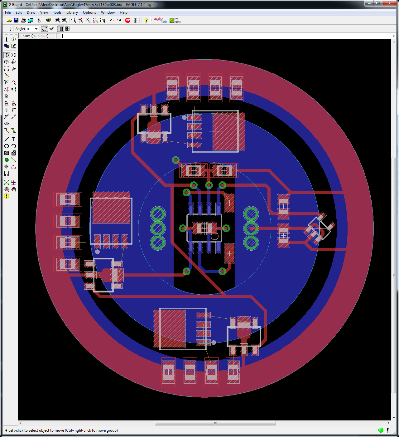
I’ve been wanting to play with this in SRK/M6 size, but I pushed that to the back of my mind since the driver wasn’t working. Now that it operates, I took a couple of hours and laid something out.
- 47mm
- MCU on the bottom. I was inspired by Mike C’s - Mod: My SupFire M6 “BMF” edition (new beamshots in OP) and the way Mike C made the MCU available for flashing.
- LDO optional. An LDO will work fine for all applications, but it costs slightly more than a diode. You can just solder on C1 and solder the diode between C1 and the empty C2 pads.
- 1.3mm LED+ vias will take 18AWG wire from the careful modder, IIRC.
- Extra pad on top for Pin 6 (extra PWM pin, temp sensor, or status LED)
- Extra pad on top for Pin 3 (probably for a temp sensor or status LED)
- OTC in case you are somehow making a clicky light…
- I’m aware the MCU GND needs to be moved. This will not be a problem.
The optional LDO is present for e-switch MT-G2, MK-R, XHP50, XHP70, etc. With the current bottom it’s intended for 8x18350 (2s4p) or similar. I think it’s apparent that the bottom copper could be easily changed to be like Mike C’s layout.
Darn this looks really good, now I’m considering rebuilding my BTU Mtg2 around these drivers. They’d be a much neater solution, and I’d imagine less thermal issues since sinking 3 large components with handy pads on the bottom is much easier/more efficient than doing the same to 48 triple stacked 7135s.
Can you put the final nail in the coffin for me by confirming that actual voltage dropout is lower or at least equal to an equivalent 7135 based board? ![]()
Cheers, and keep up the great work!
Linus
Thanks!
I only did a very small test, but Vdo seems to climb with set current for some reason. The Vdo from a bank of 7135s seemed to quickly eclipse that of the 7136-based driver as I increased the drive current (by adding 7135’s and increasing the sense resistance, respectively). I’m not sure why it worked that way. I think I wrote a very short post earlier in this thread about it.
I’m not sure about the “handy pads” you mentioned. The large pad is electrically connected to LED-, so it must be isolated from GND. If you just meant the large flat area on the top of the FET then carry on: I agree. One issue is that these FET’s are so slim that the QX7136 and ATtiny13A are both taller IIRC. Not the end of the world, there are various ways to deal with that.
Ah whoops. ![]() I wasn’t paying attention and assumed the large pad underneath the fet was for ground/heatsink. Had thoughts of mounting those fets remotely and soldered directly to a copper insert or something in the driver cavity.
I wasn’t paying attention and assumed the large pad underneath the fet was for ground/heatsink. Had thoughts of mounting those fets remotely and soldered directly to a copper insert or something in the driver cavity.
That makes it a little less ideal than I thought, I know from dealing with the 7135s that heat sinks making contact with just the top of the chip are next to useless in keeping the chip from going critical.
But again this is a massively bigger package so I’m keen to have a play around with this driver and see how it deals with the situation thermally.
Cheers
It may be useful to the wiring diagram M6.
IC U2 is something like: The ADM803 supervisory circuit monitors the power supply voltage
My M6 mod. v1 by RMM, works very well.


Technically the FET manufacturers expect you to heatsink these things through large pours on the PCB, but I think it’s reasonably common for that to not happen. I’m not too concerned about it, even at high power, as long as there’s heatsink contact somewhere on the FET package. If you look at the construction diagram (page 4) of an LFPAK56 MOSFET, it’s pretty serious in there. Big copper slabs on the inside. With the ones we are using being rated at 50-150W of dissipation (depending on the model), I think some fudging is possible.
What specifically are you referring to when you say “with the 7135s that heat sinks making contact with just the top of the chip are next to useless in keeping the chip from going critical. ” ?
Good schematic making skills aslpg!
[quote=wight]
Warning: I’m plugging in my Waffle Iron! ![]()
-
Well if you expect a 7135 to dissipate quite a lot and it isn’t soldered directly to a copper pcb area then it won’t be long until the temperature get’s way too hot at the chip level and funky things start happening (i.e going critical ![]() ). I came across this particularly badly in my BTU triple mt-g2 build where the 7135 chips at the top of the double stacks were getting particularly toasty and resulted in very unstable output/flicker not long after start up. These were the chips only connected to the heatsink/ground trace through a thin solder bridge between the two ground tabs.
). I came across this particularly badly in my BTU triple mt-g2 build where the 7135 chips at the top of the double stacks were getting particularly toasty and resulted in very unstable output/flicker not long after start up. These were the chips only connected to the heatsink/ground trace through a thin solder bridge between the two ground tabs.
In that case I tried having the top of the 7135 package in contact with a heatsink surface but that didn’t make much of a difference at all. I actually noticed that the grounding tab would be almost too hot to touch before the case of the chip was even warm.
I was just saying, that to shift a lot of heat it doesn’t make much sense to me to use the top surface of the device to do that. But maybe it’s sufficient here?
As an example in my mt-g2 light driven at 6A (with ~7v vF) from a relatively sag free 8.2-8.4v input, I believe thats over 7watts of heat dissipated per 17mm sized board, and in this case it’s all through a single component and into an electrically isolated copper trace that can’t be in direct contact with the flashlight host and to the outside of the light. Are these mosfets happy running at very high temperatures, like 100degC and up with no ill effects? I have no idea on this stuff.
I do know that with the 7135s as the temperature rises above a certain point output seems to drop off quite rapidly below the rated 350ma/380ma. Some kind of active throttling or just performance deterioration I don’t really know. If it get’s really bad then other interesting stuff like flickering and stuttering sets in. If you connect a 7135 up without any heatsink contact on the ground tab and run it for a bit you should see what I mean.
Maybe it’s not the tiny fet inside the chip that’s suffering under the heat but some of the other sense components that are also in there.
A problem solved by separating the sense parts of the circuit and the hot mosfet as with this driver design perhaps?
-
I can definitely see from studying your mosfet package that having the internals laid out like that is directly linked to the performance of the fet, both in terms of thermal and electrical resistance.
For my application in particular, but maybe for linear flashlight drivers in general a power mosfet with the large tab as the ground/source like the 7135 would seem like a far better option. Ultimately the body of the light is the primary heatsink and if the mosfet is electrically and thermally isolated from that it’s not ideal. Does something like this even exist though?
This fet may be able to dissipate silly amounts of heat like 50-150W but surely that’s not a realistic figure in this case and heavily dependent on an ideal heatsink path?
I’d be really interested in seeing a test showing how this driver responds when it has to dissipate ~3-5Watts for an extended amount of time. Seems that would be a useful power dissipation range to look at for driving an mt-g2 at over 5 amps.
I got stung by unexpected thermal issues with those 7135s so I’m probably a bit hyper sensitive to the issue at the moment ![]()
Cheers
Linus
Issues with the 7135’s when they are treated like that are pretty well known….
The MOSFETs are happy at extremely high temps. For example, the NXP PSMN3R0-30YLD should be derated to 20% of it’s full power dissipation rating when the tab is at 140°C (so that gives us 18.2W of dissipation after derating from 91W). Your PCB should be kept under 120°C though I think, or risk delamination?
The more direct your thermal path, the better. N-channel has been king for a while and all n-channel have this heatsinking arrangement as far as I know. I’m sure heatsinking to GND would be more convenient for our application, but that’s just how it is. It’s not as convenient, but we don’t get a choice about it. If you don’t want to heatsink the top of the device you don’t have to, you just can’t connect LED- to GND so you’ll need electrical isolation. I recommended potting earlier in the thread and I’m recommending it again now. It’s also quite possible to use a PCB like I posted in Post #32 and just electrically isolate it from the heatsink. That’ll work effectively to allow the heat to move into the heatsink.
Don’t look to me to do a lot of testing. Sorry.