’course I can. ![]()
Stylish!
’course I can. ![]()
Stylish!
I forget so much, so fast, it’s simply astonishing that I can look at this layout and know what goes where without even thinking about it. ![]()
Just goes to show, priorities are always a key factor! lol LOVE this driver! It has greatly eased my process and the fit into a light is so simplified it’s almost like cheating.
Peer pressure begets another driver:


[WIP] 17mm DD+single-7135 driver - single sided & Dual-PWM compatible?
It looks ready to go to me. What are we using for moonlight with a single 7135 these days? I think you posted some good info in RMM’s store thread, but I’ve lost track.
What would be cool would be if an optional 15mm daughter board with 7135 to be attached to this great piece of work which would in effect keep the bottom flat for the retaining ring. That way maybe there is the possibility of adding up 4 or 5 7135's to suit one's needs.
Mattaus already made a 16mm daughter board which carries up to 6*7135. It’s in the OSH Park projects thread. Depending on the goals that is a good option.
And how would the daughter board mate to this driver for control...and is there firmware yet that can handle it? Sort of like that 7135+FET Turbo that you have sitting around the million other ideas ( :) ) except this keeps the retaining ring side clear and you do not have to struggle to find 1/10th of millimeter. LOL
Eh, the PCB Mattaus shared is intended to be used with 1 PWM signal for the whole PCB. So you’d have 1 PWM signal for that board and 1 PWM signal for the FET. [EDIT: This should be workable with the current STAR_off_time firmware.] You would not be able to achieve as low a LL/Moonlight as you the single 7135 setup or the 6*7135+FET Turbo setup (which is setup for 1*7135 w/ PWM + X*7135 w/out PWM + FET w/ PWM).
Mattaus’s PCB uses 4 wires: GND, LED-, LED+ (just passthrough), and PWM. You airwire the whole thing together. It would definitely be possible for me (or Mattaus or whoever) to layout a pair of PCBs specifically intended for stacking, but I don’t see me doing it anytime soon.
I don’t know of any specific instances where the hybrid 7135+FET driver won’t fit where people want it to. I’m sure they exist and I wouldn’t mind hearing about them (in that thread…).
Awesome! Best of both worlds. ![]()
I don’t have a single-7135 driver at the moment, but the moon level depends on both that and on the specific LED used. Like, for an XM-L2 it can probably run at about 6 or 7, but an original XM-L may need 9 or 10.
This driver looks like it should do almost everything for almost everyone. The only thing missing is a zener, and there are other drivers available for that. I’m not really into multi-serial-cell lights anyway; my only MT-G2 light was pretty disappointing so I’m not eager to make more.
It seems that we are having some problems with Zener builds. I thought I’d tested one out on a little PSU at least, but now I’m not so sure: both DBCstm and RMM have reported [by PM] being unable to build a Zener configuration with v024 and have it work!
RMM reports that placing the cap which normally goes at C1 on the Zener pads and then stacking the Zener on top of that works. That’s pretty doable and a great way to salvage existing boards if needed.
We know the schematic to be good, the same schematic works for other designs. RMM reports that his new 17mm & 20mm drivers of similar design are functioning, so it seems clear that this is a layout issue on mine. I’ll re-test with the Zener pretty soon.
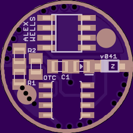
In the meantime, here’s an UNTESTED revision intended to address RMM’s suggestion of moving the C1 closer to the MCU. C1 is now fed through a single thin trace, R1 has been moved so that it is no longer between C1 and D1/R3, and C1 and D1/R3 are connected through a massive trace, and all of this is happening right next to the MCU’s Vcc pin. I also increased the size of LED+ slightly and doubled down on the GND vias. EDIT: and no, LED+ and MCU Vcc do not actually touch. It’s just OSH Park’s rending system that displays it that way.
Since I’d been playing with the layout again for this driver it struck me that what I’d really always wanted was LED+/- pads that were across from each other. IMO that’s a key aspect when it comes to very,very, tight builds. I set about shuffling things around, but they wouldn’t play nicely. Then I recalled that the LFPAK56 footprint I was using sucked. Switching to a normal Power-SO8 footprint helped, but it took me a long time to achieve the level of symmetry I was looking for. Without the OTC it’s actually really easy to do all kinds of great symmetrical patterns (ask me how I know, oops!). In the end this was the best I could do. Now that the signature look of the original driver is entirely gone, I’m not sure whether to call it something else or what.
Also note that I didn’t spruce up the Power-SO8 footprint any for LFPAK56 use. While it should function fine I’ll probably do that at some point.
As far as functioning with the Zener, this should be very similar to v030. (so in theory they both should work fine :p)
|
Oops, don’t use this one. I made a minor error with the vias & GND ring on top. While this one should work, I recommend v024, v030, or wait for v042. |
v041
OSH Park ~
Now moron’s like me can stack the MCU on the MOSFET footprint. ![]()
That looks nice Wight, dont’ think you should change the name as the Revision number suffices. That’s just me though. I’ll have to get some of these, and solder paste stencils, and give em a go. (starting to get more than I can remember what goes where) I need to use up the ones I have and switch over to these… my memory doesn’t multi-task well.
My zener build of A20DD-SO8 does not work either, normal build works ok.
Put the capacitor under the Zener, that’s supposed to do the trick.
What I don’t know is if it takes a second capacitor or just relocation of the C1.
I’m sure that relocating C1 is sufficient.
Yeah I read about that, but the C1 is half the length of the pads for the zener. Anyway I assume the layout will get fix without the need to make-shift.
I didn’t know if it needed to be there for continuity or if the pads should be jumpered or what. Thought it might be necessary to continue the lineage for the LVP.
Oops, another minor mistake. The WIP v041 version has a problem with the GND vias and GND rings. I’d hold off on that one until I can release v042, although it should function. In the meantime v024 is still fine for single cell builds or Zener w/ the workaround described above and v030 should be OK for Zener builds w/out a workaround.
No, it should be fine with C1 completely unpopulated as long as you’re doing a Zener build and have place the cap for C1 over on the Zener pads with the Zener.
Correct, C1 is not a great fit there. You may also place C1 right next to R2. There is plenty of space to put C1 Against the right-hand end of the Zener and either solder the other end to the GND ring (scrape first) or solder it to the GND side of R2. I’ve just checked to make sure it would work, I was able to solder the cap in there without an issue with the Zener already in place. Adding some extra solder will help. EDIT: be sure not to solder to the other end of R2 (the end pointed towards the middle of the PCB).
All of my first Zener mods had the Zener laying down, embracing the capacitor on a Qlite driver. Can’t see how this one would be any different.
Let me ask this then, if I already have the driver built (I’ve got 9 sitting waiting to be used) and I have need for a Zener modded version…can I add a second capacitor with the Zener? Do I need to remove the C1 from it’s original location?