The design does work, and it works pretty well. The efficiency is nice on the lower modes, with a nice glowing moonlight mode. I recommend running the 350mA binned 7135s if you want the lowest possible moonlight mode. In general, it seems like you can get a lower stable moonlight mode with it than you can with the 380mA binned variety.
For my design I had to swap the PWM outputs in the firmware, but it looks like you won't have to do that.
Would it be worth it to replace the diode with a p-channel FET? The package would be three leads rather than two, which would make the footprint a little bigger, but it would eliminate the voltage drop and thus allow a higher drive voltage to the main FET's gate (to get lower resistance at lower battery voltage). The voltage sense R's could be moved to the protected side without needing to factor in Vf of the diode. The benefits (if apparent) may only be 'on paper'.
Read this pdf from Texas Instruments: www.ti.com/lit/an/slva139/slva139.pdf
There are many others - search for "battery protection FET"
Edit- Of course at this point you may want to use an LDO...so many options...so little time to test them all. I am quite impressed at the way you've been able to pack all this into a 17mm single sided board. So please don't let my comments rattle you, this is great work! I've always been torn between making something rock solid for one specific application, and tweaking it to work in several applications. Consequently some of my designs keep morphing and never get done...
Now that you bring it up again (good time to point it out) I recall that you’ve mentioned the performance difference between the 350’s and the 380’s before. It would be neat if someone could explain why they behave that way. Anyway thanks for bringing this up.
The PWM lining up on mine was dumb luck. I was prepared to specify swapping the PWM in firmware if necessary. When laying out this design I started with the FET and moved out from there. I think this is more or less how it went, although I didn’t start saving revisions until the design was fully functional (other than vias). I try to start saving earlier but it’s hard.
place FET optimally.
place LED+ diagonally across from BAT-
place 7135?
place MCU.
fill in the rest
vias come last
I rotated the MCU a little bit and then shuffled the small components until it looked like I could hook things up. When I later realized that the PWM pins were correct I was delighted of course.
In this case I think we simply don’t have the space for an inexpensive P-channel FET. Also recall that some folks are transplanting Nanjg driver components onto these, so the less extra stuff they have to purchase the better. We really haven’t done any testing to show whether the lower resistance is worthwhile once battery voltage drops. Napkin math indicates that it’s not a big deal (eg the major limitation at that point is LED Vf).
Thanks for the link, that’s a concise and to the point article. I’ll keep the P-channel FET in the back of my mind and see if I can make use of it somewhere.
RE: actually releasing things… you see my strategy, right? Who cares if it works or not, just label everything WIP! I’m absolved of all blame!
Changed from 18x 0.5mm GND vias to 16x 0.6mm GND vias for spacing reasons.
Pulled GND via circle in a lot. The entire minimum annular ring for each via is now spaced the minimum trace distance from the board edge. This should be fully compliant with OSH Park’s design rules.
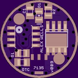
Swapped out lame LFPAK56 outline. It was nowhere near correct and just wasting all kinds of space. I used a Power-SO8 outline that came with Eagle and filled in the blanks by hand for now. I reduced the amount of solder paste laid down under the tab vs the old outline, somewhat like what NXP actually recommends. I’ll fix a real part later.
Tilted the squiggly line of vias at a rakish, dashing angle more fitting with today’s styles and trends.
Minor silkscreen changes.
I think what’s left to do at this point is pin down a name and then clean up the sloppy silkscreen on the bottom.
Wight, have you had a chance to play with any of the LFPAK33 FETs yet? I ordered some and have a few boards almost done with them, but haven't had a chance to try any yet. I put one on the 15mm version of this board and according to NXP it looks like they are pretty much equivalent to the LFPAK56 FETs.
Heh, frankly I haven’t thought any about them, although as you probably realize I have a couple on hand. I haven’t really shopped to see what’s available. Where it fits I feel like Power-SO8 is the ideal footprint since there are so many options available. It’s a very popular package and no one is likely to be unable to source appropriate parts.
That said, when I re-attack buck circuits I’ll be looking hard LFPAK33 and the other 3.3x3.3 MOSFETs. I can see why it’s a good choice for the 15mm layout.
I forgot to mention this: when I ran the CAM job for v009 I ran both the old and the new job and uploaded both to OSH Stencils. Sure enough, both were off. I think it’s just a flawed setup on their end.
As far as I can tell the dual-pwm is working fine.
Moon 2
Low 37
Med 40
with dual-pwm at 38.
Mode spacing appears to be very good set that way. I’ll build another today and post pictures, the first is in a triple XPL 3D Convoy S2 right now.
On this and on some of the DD18 SO8 drivers I am getting a buzzing on the two highest pwm modes, what normally causes that? All of the solder appears solid.
AFAIK the buzzing is something resonating. Tuning your PWM should help eliminate it. Change duty cycles (mode levels), PWM freq, or PWM type (fast/phase correct). The Dual-PWM functionality can split PWM types right in the middle of your mode group if you’d like, that may be able to eliminate the noise at the top end. That’s what’s going on with the “#define FAST_PWM_START”.
Looking forward to pics of your next driver build.
9.6Mhz is right on the ragged edge with a protection diode in place. Atmel’s datasheet shows that up to 10Mhz is OK for 2.7-5.5v, but the diode drops around 0.2v or more. So at 2.9v the ATtiny13A sees 2.7v. There may be other considerations that push you over the edge in certain circumstances.
In other words if it’s possible I’d try and stick to 4.8Mhz rather than 9.6Mhz, just to have all your bases covered all the time.
What offtime values are you using and how much time is it taking to save?