On a driver like the A17DD-S08 would it be feasible to make a copper “heat sink” that attaches to the gate and wraps around to sit on top of the FET? Glued on with Arctic Alumina Thermal Adhesive as an isolation? This would be “live” I know, but as long as it wasn’t touching anything else it would be acting to dissipate heat from the MOSFET, right?
In some of the lights I use this driver in there is plenty of room in the pill for up to 3/4” tall sink. I can see it being possible to make quite a large heat sink in copper to connect to the gate and the LED negative lead could actually connect at the top of the sink as it would be live.
Would this do any good for pulling heat away from the MOSFET and keeping it nice and stable? Some of the triple and quad builds I’ve been doing are seeing in excess of 14A.
You mean attaches to the drain? The large heatsink pad on the bottom is the drain, the gate would be a pin equivalent of the pwm input on a 7135.
It’s that age old argument of having thermal mass/internal heatsinks vs an efficient thermal path to the outside of the light isn’t it.
I went for more of the thermal mass approach on my BTU build (even though I don’t actually have to worry about isolating the 7135s electrically) and neglected maximizing the thermal path to the outside of the light. Since that is the only area that can actually get rid of the heat generate from everything inside I was simply filling up the internal heatsink and when it was full the temps skyrocketed. The fact that this mosfet is always going to need an electrical and as a result also somewhat of a thermal isolation between it’s heatsink pad and the rest of the light is my primary concern.
It may well be an unfounded concern though. I have a bunch of parts on order to put this stuff to the test!
I realize my application is somewhat extreme but if you’re dumping up to 15watts of heat into any internal heatsink that doesn’t have a great connection to the dissipating surface you’re probably not going to have a very long running, stable driver.
Thinking about it again now, I’m not really using the body of the flashlight as a ground conductor, I could probably isolate the “pill” from ground without too much hassle. That would certainly make heatsinking the fets more straight forward.
-
Wight if I have found a mosfet in TO-220AB format that hits or exceeds all the other criteria but has a “Qg” total gate charge of 212nC @ 10v, is it not even worth trying?
I’ll keep looking for something that hits all the requirements but I guess I’m not too clear how gate charge affects the situation, does it take longer to “fill” by the MCU pwm signal before the fet is fully “On” or am I looking at that completely backwards?
On a related note, seeing as there may be quite a few people planning to run this driver in a 2s configuration. Wouldn’t a zener diode rated higher than 4.3v (but obviously lower than 6v) help in any of this stuff. Certainly looking at Rds On for these fets it seems a higher voltage on the gate is beneficial, wouldn’t that also help the rest of the circuit run at a higher frequency or allow for less specific fet requirements perhaps? Just thinking out loud here…
At 212nC I think you're going to have a hard time switching it at fast frequencies direct from the attiny like we usually do.
I built a light bar where I was driving 2x external TO-220 FETs mounted on the external LED heatsink at 36V and quite a few amps. On that setup I was running a ~5.5V zener diode because I figured I needed all of the voltage overhead I could get to switch those FETs and keep them turned on fully when needed. The zener diode was obviously very inefficient stepping down from 36V, but an extra 0.5 watt of loss wasn't a concern in that application, and it was a prototype setup anyways. For a momentary setup, a zener diode is obviously not the best solution.
Cheers Richard, I’ll keep looking for a better mosfet.
Good to get confirmation that higher voltages aren’t a bad idea in this type of thing, I’ll make sure to order in some 5.5v zeners just in case.
I have some v06 boards on order, I assume the main difference here is the change to 0805 resistors and a bit of tidying?
Is the older version still fine for testing?
Looks like it. I’m looking back now… Right, I see no major issues with v006. The changes are you described. The biggest functional issue with v006 may be that the DRV/GATE trace will be partially exposed VERY close to the GND ring on v006.
Usually they come inside a couple of weeks, depends on what else is being made and how much as they fill a panel before running it. Then once it’s done they have guys separate everything and they ship immediately after that.
I know the feeling, I ordered mine on Dec 28th, shipped Jan 8th so hopefully they’ll be here soon.
It’s sad having all the components on hand but no boards in sight.
I just got my shipping notification. 3 each of the 20mm and v06 17mm. Exciting stuff! I hate the look of all the 7135’s stacked, so hopefully this will be the solution. :party:
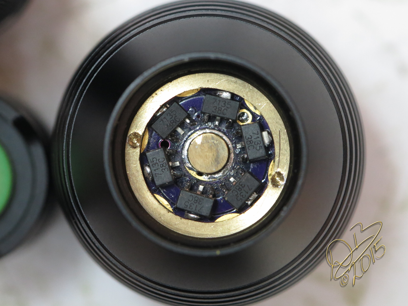
You say you hate the look of stacked chips, have a look at this board and tell me which ones are stacked….one is the moon mode, the others are the rest of the modes. Wights PZL driver.
Love how this looks in the tube when changing cells!
I’ll take a guess! The top left corner is not stacked.
a deeper pill with a retaining ring like the x6 makes it look fine, but sticking out the bottom of a P60 is ugly to me.
I sat there and looked at it, very pleased with how well the stacked ones blended in. Really it only shows in that center leg that isn’t soldered. The stacked ones show the center leg bent down.
I hear ya, whenever possible I used to do all the stacking on the inside. Seems like I had 22 chips on a board before. Chips everywhere. No Coke, Pepsi….
Don’t forget that you’ll need to significantly drop the PWM freq for this thing to work correctly. The last test I did was at ~1khz I think. I switched the firmware to Phase Correct PWM and used the :8 divider as per post #51 in this thread.