Oops, another minor mistake. The WIP v041 version has a problem with the GND vias and GND rings. I’d hold off on that one until I can release v042, although it should function. In the meantime v024 is still fine for single cell builds or Zener w/ the workaround described above and v030 should be OK for Zener builds w/out a workaround.
No, it should be fine with C1 completely unpopulated as long as you’re doing a Zener build and have place the cap for C1 over on the Zener pads with the Zener.
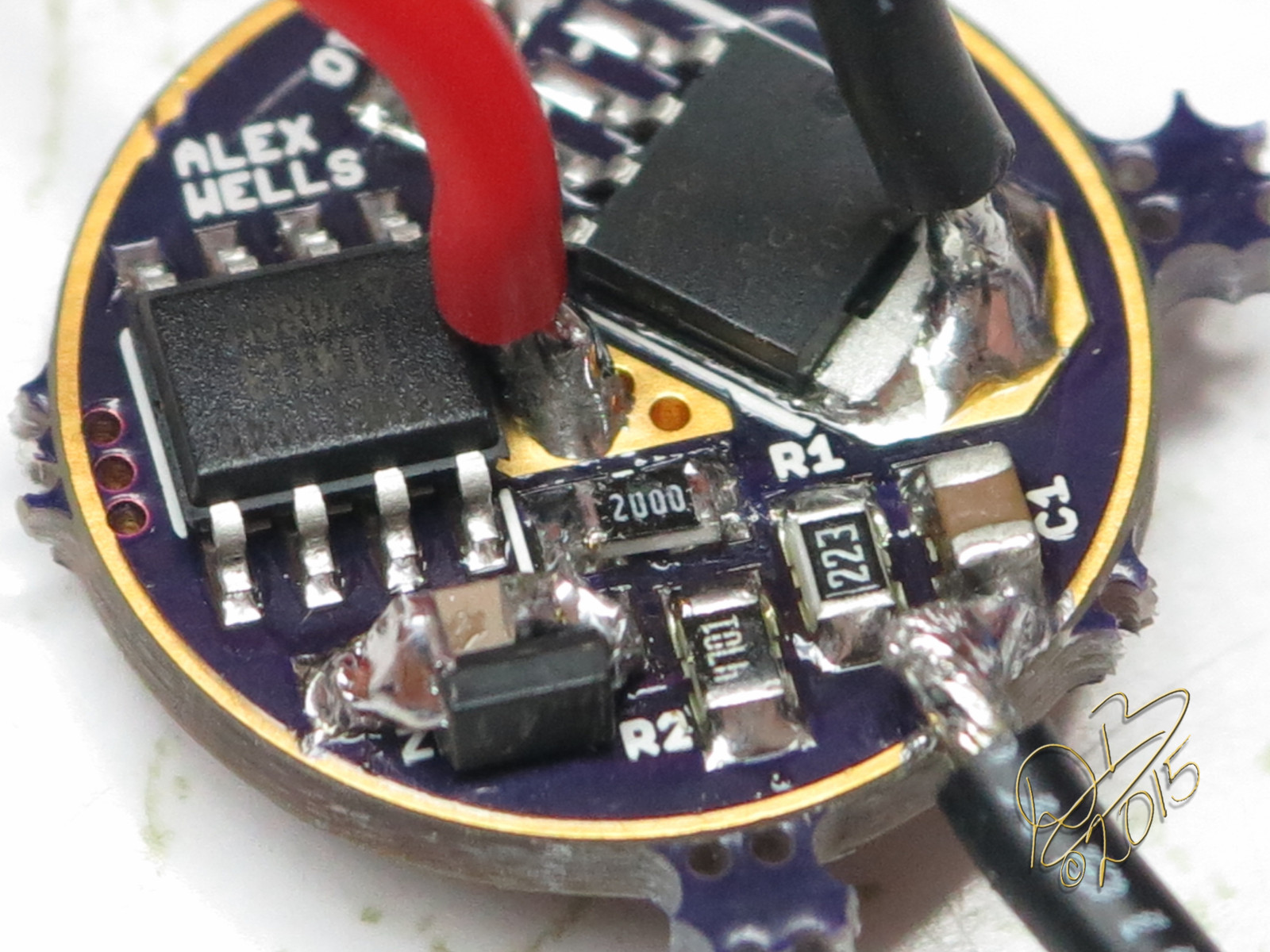
Correct, C1 is not a great fit there. You may also place C1 right next to R2. There is plenty of space to put C1 Against the right-hand end of the Zener and either solder the other end to the GND ring (scrape first) or solder it to the GND side of R2. I’ve just checked to make sure it would work, I was able to solder the cap in there without an issue with the Zener already in place. Adding some extra solder will help. EDIT: be sure not to solder to the other end of R2 (the end pointed towards the middle of the PCB).
Let me ask this then, if I already have the driver built (I’ve got 9 sitting waiting to be used) and I have need for a Zener modded version…can I add a second capacitor with the Zener? Do I need to remove the C1 from it’s original location?
I think it’s different. When I set a cap on those pads it looks a bit tricky to solder in place. The cap can’t touch both pads at once - the SOD123 pads are too far apart. Your Qlite builds had a 0805 cap sitting on a 0805 pad which is longer than the cap itself. The SOD123 Zener will actually just barely fit on long 0805 pads by itself…
Good question! The answer should be no problem. Add the cap, leave C1 in place, and you should be fine IMO. I’d bench test to be sure though.
I wasn’t going to do it tonight, but my curiosity made me look at it, and from there I was a goner.
Piece of cake. Took a built A17DD-S08, removed the diode, stuck a 200 ohm resistor in it’s place, held the small capacitor between the pads with needle pointed tweezers and touched solder to the pad then the cap, same on the other side… cap in place. Located the Zener for position, laid it on it’s side cupping the cap, badda bing badda boom done!
Soldered on 2 20ga leads, stuck those to a 20mm Noctigon with an MT-G2 on it, soldered by ground lead from my test cell that has a switch soldered to the negative, taped a second cell to it. Fired it up! 5 modes, presto! :bigsmile:
Thanks Guys! Really appreciate it, that was kinda driving me nuts! My last 2 Zener mods I went back to the very first BLF FET boards from matt, out of retaliation. lol
Looks good. Thanks for posting the pic showing how it’s done!
I think making that joint is probably fine for those with enough soldering experience (and a pair of tweezers ;)), but some might find it difficult. The alternative placement I mentioned above also works best with a pair of tweezers, so I don’t know if it’s any easier.
I’ve only been soldering since I got the Hakko 888 station. I used to butcher stuff horribly with a 25 watt Weller iron or an old Sears dual power gun. I sucked, in very ugly ways with cold joints that broke.
So I’ve only really been successful for about 6 or 8 months. Might be close to a year now, don’t remember for sure. I DO remember that switching to the .031 solder helped tremendously even before the Hakko, then getting the right tool made all the difference in the world.
I’ve used a small variety of soldering tools. For years I used a 100W gun for everything (do not do that). I’ve had a 25W and a 40W iron IIRC. I also have an 80W iron for use on big, stubborn things. Eventually I got OK with the 40W I think. Then I got a knock-off temp controlled station. That was an improvement, but after 6 months or so it started having problems and within a year of purchasing the knockoff station I got a Hakko FX-888. I’ve been very pleased with the FX-888.
Updated top silk w/ L+/- identifiers & orientation mark for MCU.
Updated MOSFET footprint including tstop and tcream. Tcream isn’t perfect but it’s better than the old version (which put down way too much).
Updated spring bad on bottom. Main circle is exactly 8mm, the spurs extend to 11mm (for soldering on a 10mm spring). I’m still open to suggestions about what spring sizes people use.
Moved the lone via closer to center of board. Via is now w/in 0.5mm of being centered.
Updated bottom silk to fit new spring pad.
The via being 0.5mm away from centered is bothering me. I’m aware that I can improve the appearance of the bottom by rotating the spring pad & silkscreen a little more. That will likely happen in a future version.
Seems like moving the OTC to below the Zener should allow that via to be centered. The OTC trace would have to run between pins 7/8 edit 6/7 and the OTC pads would have to straddle the pwm trace but neither of those are untried.
Edit: Before I do….if you’re gonna make any changes, is it possible to open up that center via enough to put a 22ga wire in it? Plug a wire in for the spring bypass and deliver current straight through the board to the needy side
Wight, you've really outdone yourself here with this driver--it is really that great. Those spring solder points are pretty cool. I know now how much time it takes to design and tweak these things, and even though I know you're faster than I am, I'm guessing at this point it is a 40+ hour design. Bravo!
I just ordered some of these 043 boards and stencils to go with them. Wanted you to know the stencil layout looked perfect! Looking forward to getting this one in, like the PZL it should look really nice installed in a light.
Fortunately for my sanity Eagle doesn’t seem to have an hours counter on my files. You’re right, I have a significant time investment into that layout. There’s approximately one component too many involved: I was easily able to create nice symmetrical layouts when I accidentally left a component out.
You’re right of course. This entire design was done with two considerations in mind:
diagonally opposed LED+/- at the board edge
some semblance of symmetry
So I can’t get away with moving the OTC there. This final iteration (there were many in between v030 and v041 - I only iterate version numbers when I save, and I only saved during that process when there was an idea I wanted to preserve) started with a component in that position and a hard battle was fought before R1 and R2 lined up at 90 degrees vs the rest to allow everything to fit. More hard battles were fought after that of course since everything failed the DRC if I recall correctly.
If enough space can be freed up to get the via centered and larger that can probably be done. In the meantime there’s no reason not to drill it out: just be sure to solder the top (component side) when you feed the 22AWG wire through the drilled hole.
Great! I do really appreciate pics of people’s builds, from the driver to the rest of the light.
… and BTW here is an unattractive (to me) v044 - OSH Park ~
As you can see, the central via has been moved again in order to center it on one axis in relation to the silk and exposed copper. The entire central medallion area is still skewed with relation to the B+/LED+ vias. IIRC those guide rings are for 11mm, 8mm, and 5mm… or something.
I plan to take that back to the drawing board and:
continue to think about how the central via can be handled
fix the skew on the bottom
re-do the spring pad like v043, but with a thin, solid combo guide ring for 6mm /5mm in the middle of the 8mm pad.