I think jotting down observations on a piece of paper seems much easier than burning time searching for library elements for an unknown MCU and other components. Maybe for a more complex circuit, but for our drivers a sketch seems adequate.
Would be nice to document all tidy and all for future reference though.
One factor is how well you understand the circuit to start out with. The better mental image you have of the circuit, the easier it is to draw in either format.
There’s no reason to go running around looking for library components. Just pick something that uses the same package and go with that. It’s not like someone is going to flip a power switch on your Eagle schematic: it’s just a representation. More experienced Eagle folks may normally just make any missing parts, but I don’t usually bother for a schematic.
Number of components that will be swapped over is 15. Actually, 13 swaps and 2 additional components (EEPROM and a 30K resistor) will be added. Six of the ten swaps will be resistors, three the colored indicator LEDs, then the MCU, EEPROM, thermistor and the tantalum capacitor. I'm not crazy about tantalum capacitors, but since it is part of the MCU's and the EEPROM's power supply circuit, I will error on the side of caution and swap it over.
Heaps of air wires will be needed. Some traces will need to be cut and new "traces" laid down for the indicator LED's. They are feed a positive charge from the MCU on the KD driver, but a negative charge from the MCU on the HD-016.
If I was handy with Eagle and Gerber files, I would make an adapter PCB for the MCU. Well, maybe not. I don't think I would want to wait for an order to be fulfilled. I'll air wire and secure wires/mcu/eeprom with a little silicone.
I noticed my diagram does not show the tantalum capacitor connection to B-. I will eventually make a nice diagram for future reference and post it. I'll try to do it in Eagle.
Hi, I’m new to his forum and first I would like to thanks ledoman for his great review of this light, ImA4Wheelr for his reverse engineering job and others for their contribution to this thread. I’m engineer in electronics, hobbist and embedded systems programmer, and I’m the recent owner of a HD-016 from Gearbest that I bought for my mtb. I’m very interested in modding this light, and I would like to add my “little grain of sand” to this thread. It seems to me that the stock MCU is an Attiny 24, (VCC and GND pins match Attiny pins, OC1A and OC1B, (ATtiny PWM outputs), are tied to led1 and led 2 PWM controllers, maybe Aref is VCC and not internal ref…), so maybe the best solution would be to reprogram the stock MCU using ISP pins. I will try to read it’s firmware,maybe it is not protected, but even if I couldn’t, it would be very easy to program a new custom firmware.
This weekend I will try to make some photos of my semi-modded light.I have improved thermal dissipation using thermal compound and two pennys attached to the back of the pills.
Ledoman, I like your idea of connecting both pwm’s in parallel and use a combination of Rsense’s, but I’m not sure if current regulation will be stable. I will give it a try.
Jose Luis, welcome to the club ;-). it would be nice to have some EE here helping us (and yourself) solving electronics issues. We are mostly lack of that knowledge.Please see my post 100 with plan of another driver with same user interface as KD2 driver has and there should be the same chip IC4 regardless it is a boost driver.
Please rethink about my idea using both output circuits combined. Probably there can be some interference, but since there should not be any PWM this should not be an issue. It is just if the current from one circuit can interfere to another. Diodes should prevent that, but please take a closer look. Thanks. Of course I would also use different sense resistors in the case this idea should work. This would eliminate a lot of hassle to reprogram IC.
Hi, I have tried to communicate with MCU by using both TPI and ISP modes, but with no luck ,may be it is a PIC, and I have no experience working with pics, only with AVR’s. Next step will be combining Rsense resistor and put leds in parallel, but I need to find SMD resistors with low values.
^ Yes, it's been progressing slowly partly do to it's complexity and partly due to lots of life interrupting events. I haven't had a chance to mod any of my lights in ages. When I do get a chance, this project get the attention.
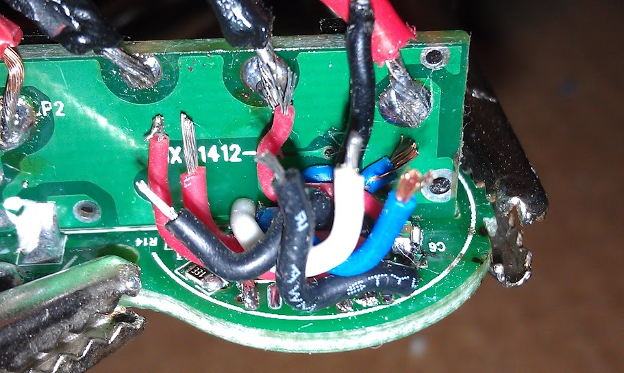
I'm hoping to bring the frankendriver to life tonight or tomorrow. I'll be honest. I'll be holding my breath. I've never so massively changed a driver. The MCU's have the same number of pins, but that is the extent of their commonality. For instance, the KD MCU feeds a positive charge to the indicator LED's, but the HD-016 MCU feeds a negative charge to them. The forced me to cut traces and wire in new circuits to keep that functionality. I wouldn't be surprised these two MCU are from completely different companies.
Anyway, I hope to be reporting good news and updating the OP with all the mods that have been made to the light by the end of this weekend.
Things are not going well with the MCU air wiring and I will be ditching that approach. Keep running into complications. There are 12 needed in total. Below is second attempt before the blue wire in back broke free and I gave up air wiring this MCU. Thinner wire would help, but still be problematic. Please ignore the sloppy LED lead solders on top. I just tacked them to have load testing purposes.
Garry is being very patient with my pace on this light and has OK's me going with an adapter board. So I'm finally going to learn how to used Eagle and make Gerber files and such. I don't know what MCU I'm dealing with. I think I will just build the element from scratch based on dimensions. If anyone has any tips for a better approach, please advise.
Thanks ImA for all the hard work! As I stated via PM, I never expected this mod was going to be so difficult and frustrating for you. Keep up the good work!
I didn't either, but it's all good. I'm learning things that will be useful in future projects. That is part of why I want to do this mod.
Looks like the PIC16F676 may have the same footprint. Trying to verify and see if any of the major vendors have a library part for it. The SO-14 in the Microchip library looks like it may be a match.
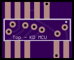
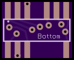
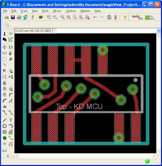
Critiques please on this SO14 MCU adapter board. Eagle has been kicking my butt all week. Not a very intuitive progam and I kept having issues with mirroring, routing, and just being a dumb ass. I finally have the following built. I think I'm at the point I build Gerber files. I don't know why I can't get a yellow "X" on the far right via. I have check and double checked several times. Any possible causes or other recommendations appreciated. Here are pics of the combined and individual layers.
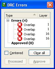
I ran a routine called DRC and it gave me the following. I don't think I need to be concerned about any of it, but I really know nothing about Eagle yet. All the errors seem to be at the via's. Maybe from me trying to make smooth traces? Please let me know if there are any problems I should fix. Also, if there are any other routines I should run.
Ended up rerouting everything. Got rid of almost all the errors. Don't know how to get rid of the error for the 2 pins that happen to be directly on top of each other. I put via's on the contact pads to electrically connect them. Not sure if I need to fix the errors. Gonna post a question in the Eagle thread. Here is the latest:
Those yellow crosses over the vias are not desirable, at least not when I do my boards. They might not really matter, but they are an error indication from Eagle. If you have the signals routed correctly, these shouldn’t show up.
Regarding design rule checks, many people don’t do them at all. They do generate a lot of errors that are of no real concern, like the overlap in your last post. It’s OK to put a via directly under a component leg like that, but eagle flags them as an overlap error. As long as the signal is the same it’s no problem. Another error of no real concern is when vias of the signal are close but not under a leg. You might get a clearance error. Once again, if the signal is the same it is of no concern. Stop mask errors are also no concern. You get them when there is white print from a component that crosses exposed copper, and OSH Park (I guess most other manufacturers too) don’t care, they do not put white print over exposed copper.
Personally I always do design rule checks. I do them once I’m close to the end of my design and I go through each error. The errors I don’t care about I approve, and then they don’t show up in the list any more unless you move the component or trace that caused it. It doesn’t take much time to analyze and approve them, and by far beats the headache of having missed something. I’ve been saved a couple of times when the DRC found sloppy mistakes I didn’t notice myself.
Download the manufacturers DRC files. Eagle’s default design rules are not the same as OSH Park, like drill sizes for vias for example. If you’re going to do a DRC you might as well do it using the design rules from the PCB manufacturer you will be using.
I also have downloaded OSH Park CAM files for gerber generation. If I remember correctly, there are different CAM files for different versions of Eagle. There are newer CAM files for Eagle v7.2.0. I don’t use the ones Mattaus provided in the Eagle tutorial thread as I use Eagle 7.2.0.
Wow, lots of excellent info there. Thank you. It all sounds good to me. I will follow it.
Yeah, I eventually figured out the X's were bad. I was pre-instaling the via's, but only on one side. I eventually read about using the shift, mouse click function. Then did it on both sides and the error would go away.
Finally got the adapter board designed and ordered. It took me a lot of time. I struggled with learning Eagle and building the parts. Parts represent the MCU’s. I could not find any already made as I don’t know what MCU’s these are. I ended up having to manually make a mirror image of the part the represents the HD MCU and then use the Eagle Mirror command to get it on the bottom side of the board. When Eagle did that, it put the pins in the proper spots (not mirror image). Anyway, I spent a ton of time on the whole process, but I can now design my own custom pcb's. That is going to be really handy for me since I tend to swap MCU's in drivers. Special thanks to Halo..., Mike C, and wight for the tips they provided.
I'll report back on weather they work when boards come in.
Here is an idea of what they have under the solder mask.
A tip about library parts, especially for MCUs (maybe a bit late). You don’t have to know the exact MCU to get a library file for the footprint, you just need to know the case. The one above looks like SOIC14. So to get one create an account at Newark Element14, find a SOIC14 processor (like the ATtiny24) and there is a CadSoft_EAGLE link under the product information:
There is a readme.txt in it describing how you make a library part from it.