I like the flexibility of still having the LED+ pad. Using the bypass hole is better for performance, but I personally think it’s less convenient, so I’ll probably only use it 20% of the time.
Anyways I cleaned up Rev2.1, so it should be ready to go if someone wanted to order it.
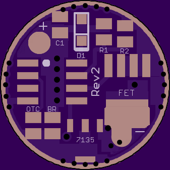
Your upgrades look great. Lot more copper and nice looking lines. I meant to say the first time that I really like the way you organized this driver. Very few long traces. Gonna have to order some next time I place an order.
I don’t like using adapter rings or piggy-backing drivers unless I absolutely have to, so I stretched this out to 20mm and 22mm, and added some features.
20mm and 22mm are identical except for the outside diameter. They have all the same features as the 17mm board, plus:
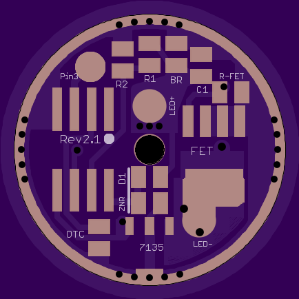
Good news! My order of 17mm Rev 2.1 boards came in today.
When you’re staring at a computer screen working in Eagle, it’s easy to forget how tiny these things are. It’s good to get feedback of exactly how Oshpark is going to produce what I’ve drawn on a screen. Overall I’m very pleased, but here are a few notes:
Notes:
My Turnigy 20awg silicone wire from RMM fit’s just fine in the through-hole, but anything bigger is a no-go. I’m glad I didn’t make the hole any smaller
Everything is a little closer to the edge than I was expecting. There’s still enough room that it shouldn’t be a problem, and I think it is partially Oshpark’s fault (a few things are wonky)
in future designs, I’m going to expose more ground ring on the top (I’ve already done this on the 20/22mm boards)
small fonts and Oshpark are not friends, so some labels on the board are hard/impossible to read
these will work just fine, but next time I’ll make the LED+ pad and FET pad bigger, like Wight did.
D1 is only used if you are actually using more than 1 cell, correct? Also, does it hurt anything to populate the bleeder resistor if you do not have a lighted tailcap installed?
One of the D1 pads has a rectangle around it and is next to the outside ring of the driver the other solder pad has a square around it and is more toward the center of the driver near an MCU pin.
The diode does not connect to the ground ring. The end nearest the ring is actually connected to batt+, and the other end connects to the mcu pin it is closest to.
Nope. Backwards. The cathode, which is marked with a line on the diode faces the attiny.
The inside line making up the “square” is suppose to be the line indicating cathode side.
Instead of a rectangle around one pad and a square around the other pad, you’re actually suppose to look at it as a rectangle around the whole thing, both pads, with a line toward the cathode side.
At this point the only thing I would change would be to make the labels a bigger font, but I don’t have any plans to do that right now.
I technically haven’t tested a built driver yet (haven’t had time) but I have checked continuity on the pads with my DMM and everything seemed correct.
If all goes well, I will have one built and tested this weekend. I may only use 2 7135’s on it since I do want it to have a good low ML mode. I will be loading it with a modified version of the BLF-A6 firmware with the blinky hidden modes removed, leaving only TURBO and BATTCHK. I do like going directly from ML to TURBO, so that got left. If I get time this weekend I will run the battchk firmware and will test the LVP on the driver. I am using 22.0K resistor, I do not have 19.1K and did not feel like a separate Mouser order with shipping for 10 or 20 resistors.