I’d suggest testing the transistor prototype then do a gb. Tape the boards to an index card and use small photo mailers to keep postage costs under $1 per set. Over seas mailing 1st class letters(which photo mailers qualify as if kept flat) isn’t much more but delivery is suspect to certain places. Other shipping options are more secure overseas but price goes way up. You’ll see what I mean when they quote shipping on that $10 order.
A groupbuy is probably a good idea. I’m hoping to get two versions going, one with a pot and/or a slide switch, and then the version with the transistors. (although pyro and Djozz will probably beat me to it)
THanks for bringing up shipping costs
Texaspyro has much more experience with this so I suggest you check out his leads. GB’s are a pain but a big part of what makes this place special so I’m glad when someone steps up to get it done. Sort of a pay it forward thing.
I have also used gojgo.com and they do have pretty good service and excellent prices if you are doing bulk stuff. I perhaps incorrectly assumed that you were looking for ~10 boards, but if you are doing hundreds it is usually a better deal than seeedstudio or a lot of the others.
Be extra careful to make sure that your solder masks, etc., are correct because there is no preview and if there is something that is a bit off you may be surprised with what you get back. Check and double check your stuff before you send off a large order (I know this from experience).
I verify my files by downloading them to OSHPARK and then send the .BRD files to gojgo/dirtypcbs. Both places can work with .BRD files. dirtypcbs provides some basic preview images.
More good tips, thanks.
That would be my big worry about a large group-order, that it would come back wrong and it be my fault :~
So yes, Richard, I was orignally thinking about a small order.
Has anyone tried this board?
MTN-17DDm 85 v0.1 BETA
I am confident on RMM skills :bigsmile: , but as he labeled it as beta version, i would like to read any opinion.
Thanks!


I too have been working on a similar board.
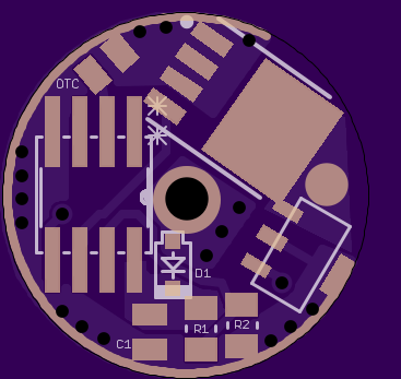
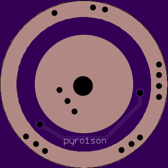
Hi pyro1son,
i like a lot how you have connected atmel pin and 7135 vcc through a vias, this way would make RMM board traces neater.
But, aren´t some components in your desing too near of the board border? what is the max diameter?
From my recent experience, an EE advised me the cap (C1) should be after the diode. I think from looking at these 2 designs, The MtnE one has the cap before the diode, while the pyro1son design has it after.
Edit/Update: 2 technical BLFers said there is a good reason for having the cap before the diode, and there's history on specifically choosing to put it before the diode, so I am confused, but leaning more for it being before the diode like in RMM's design...
Seems like the 25/45/85's are more sensitive to noise issues, maybe on the v input. They are having troubles with multi-LED high amps with FET PWM's. On the 22mm wight FET+1 board, I used the zener pad instead of the C1 pad, and seems to work out better - the zener pad is after the diode and closer to the MCU pin.
I too though am concerned about the board edge clearance - fine for some mods, like piggybacking, but may be a problem for typical driver shelves.
Edit:
I posted this over in the 25/45/85 thread as well, maybe more exposure here?
I just did a little research on the D1 and C1 positioning. The original Nanjg 105C and Nanjg AK-101 have the cap after the diode. Also an old BLF DD driver I had was like that as well - cap after the diode. But with BLF DD 1.0, the cap is before D1 and from then on, seems like we kept it that way.
Anyone have any ideas on this? Maybe it didn't have any effect at the time, and was easier to layout?
It’s definitely easier to layout that way, for me at least. I didn’t know it would make any difference though.
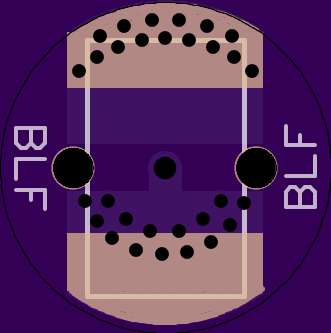
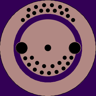
Cajampa asked me to draw up a switch PCB for the sole purpose of having the least resistance possible. This is the result.
- 16.8mm OD
- 10mm Spring pad
- (15) 0.7mm vias per pad
- Large 1.15mm via in the center for easy soldering of spring-bypass wire
- 2mm holes on either side in case you still decide to do a total pcb-bypass
- Outline on board is an Omten 1288
Hopefully this makes Cajampa as happy as the PCB appears to be ![]()
Such high frequencies may not be a problem here, but for some circuits, interference is reduced by making more of the board copper, even where not needed for lower resistance. That is from the capacitance between the sides of the board. That also helps with heat flow. On the other, hand, narrow traces to the control unit might protect it with their resistance and possibly their inductance.
Thanks for the explanation Tom E, it is good to know.
Thanks, Yeh probably still working in it I have a version that uses 0603 parts and that’s fine
Yeah ![]() thanks for doing this PD. Very nice to get pre done bypass holes also.
thanks for doing this PD. Very nice to get pre done bypass holes also.
Feels great you having taken the higher amp capable switch board to the logical BLF end game. As we realized with Dale’s testing of the lighted version and his bypass of it, the gain is a possible little less than one % but if we don’t want lighted tailcaps in a build why not get a max amp one instead ![]()
And love the grin design, it grins just as much as i will when i put it to good use knowing that perfectionist pleasure that the switch pcb is pushed as far as possible, in lowering resistance and minimizing that precious volt drop to the high Vf cree led we all like to use in our brightest builds :bigsmile:
Fritz t. Cat had an interesting point above here about lots of copper in the boards, i think it is likely that these higher amp switch boards should reduce switch failures by being better heatsinks for the switches also.
Updated post #1605 above with a note. Hope RMM can help clarify - think he might know some bout this.
I hope RBD updates the OP with these latest items.
Just a suggestion but the highest source current occurs at the fet so the most gnd vias should be there, next is the 7135 source, then the mcu, and lastly the voltage divider and OTC so the vias should be allocated accordingly. Most drivers seem to be designed with only led+ given high current capability forgetting that single sided drivers often need to get current to B- through the bottom of the pcb. Glad both you and Rich are paying attention to this.
I’ve caught up on adding links to the op. There are a number of projects out there on the forum that aren’t listed partly due to their prototype nature and also due to my reluctance to mine the forum for these things without their creators stated approval. If you’ve posted something and I’ve missed it or wish something to be added go ahead and list it here or feel free to wack me with a pm.