Thanks Halo for the research. The stacking of 2 of the 22 uF's may be a good option to try on the std wight FET+1 17 mm driver.
Just glad I got the M6 mod working well for now. The problem may not be an pronounced on the 17mm board. Dale is the only one that reported it.
Possible side effect -- last night I was re-flashing the 85 with the driver fully wired up in the M6 head, no batteries or external power source. When I'd plug in the USB dongle, the flashlight would do it's 2 blinks for power-up, then when programming, the light would go nuts in flashing the LED's. Wondering if the bigger cap is causing this? Also had a few verification errors at address 0x200. Finally got past it after a few attempts - dunno why that's happening now as well.
Update:
Problem came back - few times in a row, power resets etc. - still happened. Let it sit for couple mins, then it's working again. Huh?? Jury is still out - maybe heat related? But can't pin it on heat just yet - I got it even hotter afterwards and can't reproduce the problem. May need different/better cap solution - maybe Halo's recommendations. Might be worth investigating differences, etc. Maybe DEL's suggestion on the resistor and 0.1 uF cap, etc....
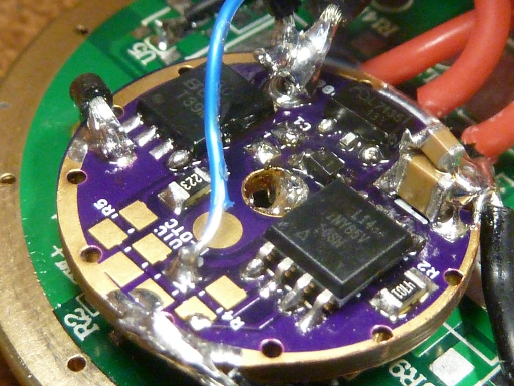
Since the emitter +power does not pass through the driver board, you can try to replace the 24 AWG wire with a 10 ohm resistor. Together with C1 this would create a low-pass filter for the power feed to the driver board. I would use 1 uF on the zener pads. The intent of this local decoupling capacitor is remove high frequency switching noise, mostly created by the MCU itself. Ceramic caps are much more suited to this than electrolytic. The ‘standard’ value here is 0.1 uF, but 1 uF may be more appropriate in this case. C1 at 10 or 20 uF should be sufficient. Keep in mind that C1 is located just beside the FET and depending on the capacitor type may be severely affected by heat (not damaged, just temporarily much lower value than nominal).
From your tests it seems the MCU is flaking out before BOD is triggered. The 85V is rated for 1.8 V up to 4 MHz. Can you test at 4 MHz? And also test 8 MHz with BOD at 2.7 V?
The bigger question is why does this only happen with hi-current cells and high current draw? It points to a ‘high’ resistance somewhere in the power circuit. Try to draw out the power circuit and think of ever wire, solder joint and PCB track as a resistor. Not familiar with the original driver board serving as ‘motherboard’, but I would look very carefully at the PCB traces and where you tap the power for the retrofit driver from.
Re. the flickering emitters during programming, if you still have the diode bypassed you are back-feeding 5 V from USB to the emitters+. This may interfere with the programmer.
Ok - this is all a huge help DEL. Yes - still have the reverse polarity diode out, wow - good to know, I'm sure then putting it back will fix it... Not sure bout testing at 4 Mhz, not sure what's involved.
I'm gonna do more tests though with putting the bigger cap(s), like 10 uF, on the zener pad - just the relocation might help. Right now, the C1 pad is before the diode which may make it less effective. Maybe should be on the MCU side of the diode to be better?
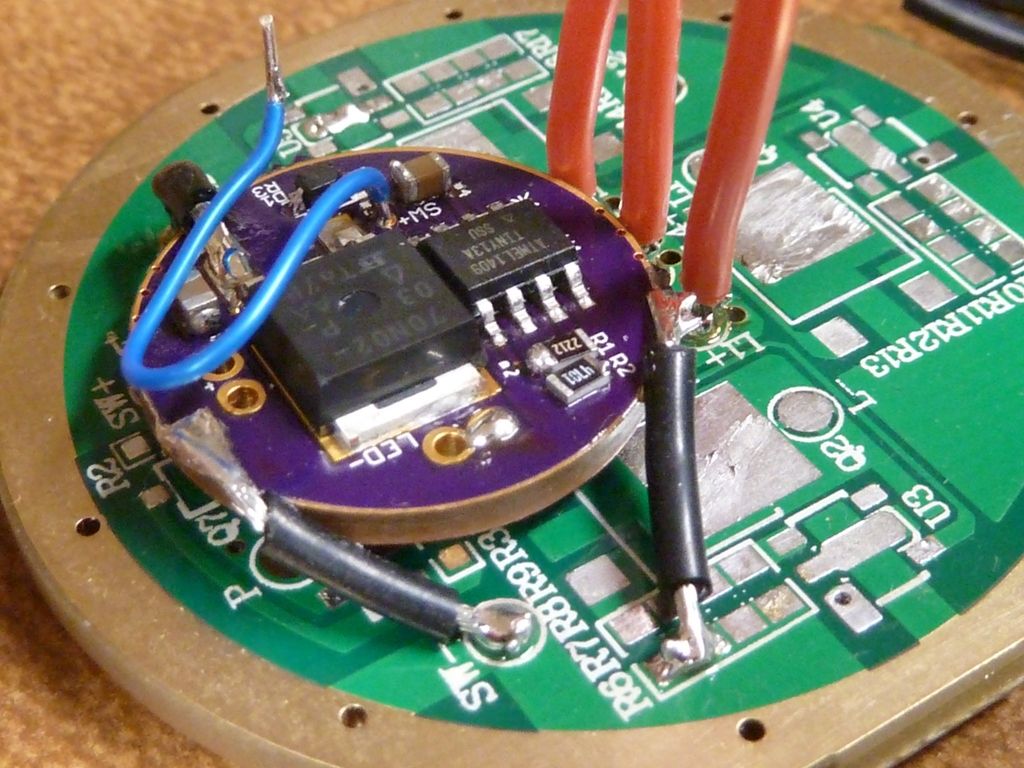
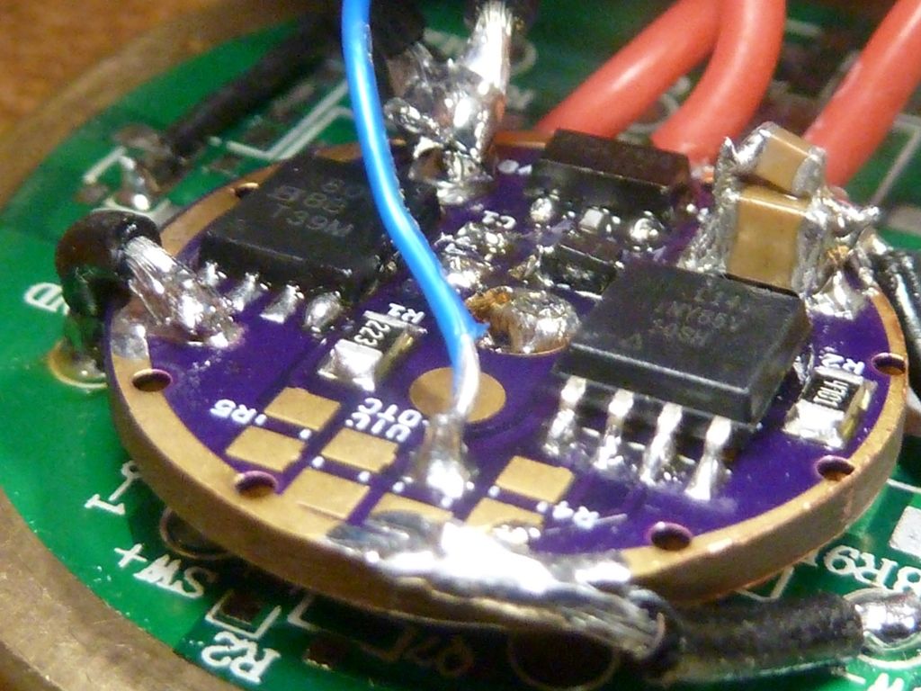
For the driver - here's a pic of the orginal mod (not now):
I simply replaced that piggyback'd driver with the new 85 based FET+1.
The usual thinking for decoupling is to have a smaller value capacitor millimeters away from the consumer and another larger value capacitor 10s of mm away. In this case the roles would be fulfilled by Czener and C1 respectively. The idea is to have a low inductance connection to the first capacitor. For this we need short or no tracks and a physically small capacitor.
D1 complicates things and we may inadvertently create some kind of charge pump. Will have to think about that one.
4 MHz should be easy…different fuses…#define F_CPU 4000000UL…and adjust _delay_loop_2 if you are using it. PWM will be half speed of course. And the clock will be outside factory calibration for the same reason as running the 13A at 4.8 MHz.
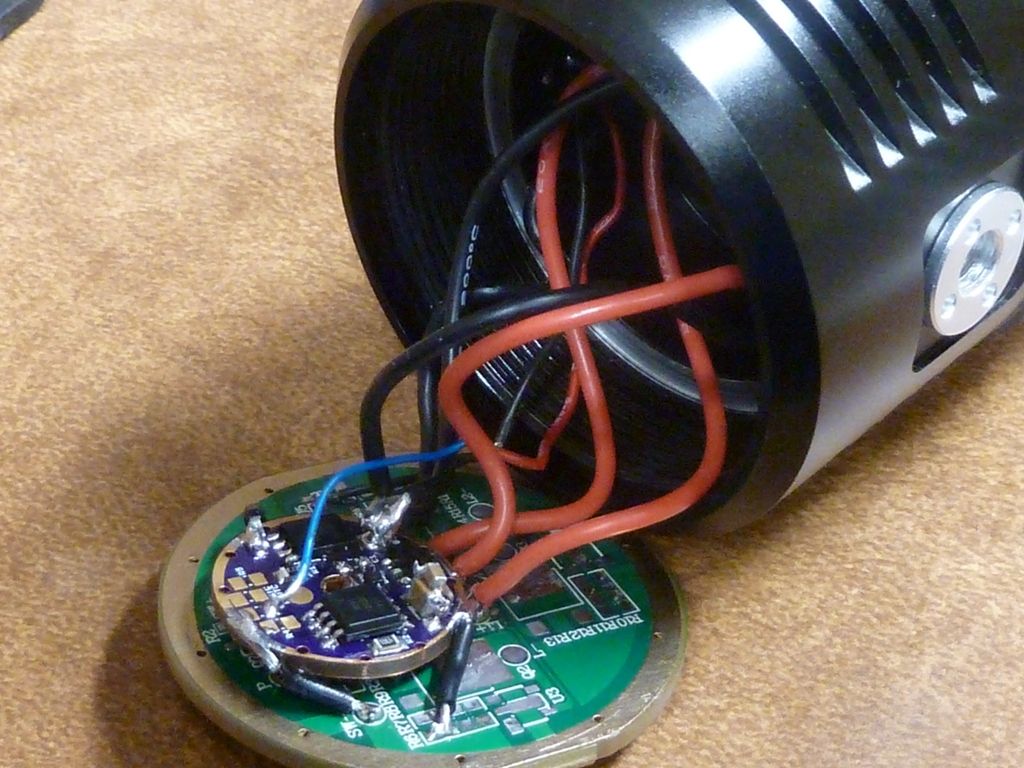
Looking at the photo there is potential for a ground loop. Test bringing only one ground wire to the driver and bring it to a point close to where the MCU takes its ground from (close to R2).
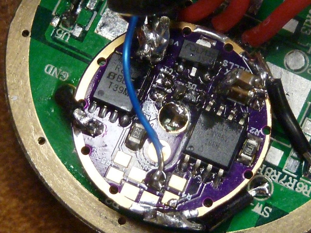
I just did a little research on the D1 and C1 positioning. The original Nanjg 105C and Nanjg AK-101 have the cap after the diode. Also an old BLF DD driver I had was like that as well - cap after the diode. But with BLF DD 1.0, the cap is before D1 and from then on, seems like we kept it that way.
Anyone have any ideas on this? Maybe it didn't have any effect at the time, and was easy to layout?
Putting the cap after the diode can cause the CPU voltage to rise to unacceptable levels. Inductive spikes get stored on the cap, raising the voltage. The cap can’t drain back into the (low impedance) battery because of the diode… the circuit behaves like a boost converter. There is a thread that talks about the issue…
I agree with texaspyro about the boost converter effect. This is the ‘charge pump’ I mentioned above.
A safer option would be to keep the bulk decoupling at C1 and just use a small capacitor (0.1 - 1 uF) on the zener pads.
There is normally nothing to gain by moving all the capacitance to the closer pads.
I looked briefly for a reference, this one seems as good as any and actually refers to boards without power planes like our drivers:
The larger capacitance may be a band-aid on the real problem….there seems to be an excessive voltage drop somewhere during high-current PWM. If this is the case then you will find that the C1 capacitor is useless because it will be loaded by the emitters during these voltage dips. This is where a 10 ohm or so resistor in series before C1 may help.
Hhmm. Looks like comfy and wight didn't agree on this issue. Yep, a lot of history lost... Wight says in Post #1068 exactly the same thing an EE told me - "put capacitance very close to sensitive but low-draw devices". Neither seem to know enough of the theory, or have enough experience, but they certainly know more than I do.
DEL is probably right - maybe just adding the small cap at the zener pad would solve it, and keeping the original 10 uF at C1 - didn't try that unfortunately.
Thanks TK - saved that link. comfy had some invaluable pics. It may not help some of his better posts/threads though - really can't tell what's goin on - he used pics heavily.
OK - made minor tweaks to my e-switch firmware. Changed 2 timeout values because I think the timing was better:
After some more talking about it here @work, even though it's working now with the caps after the diode, I'll move the 2 caps (22 uF and 1 UF) before the diode. There is agreement here about the charge pump effect, so it's a worthwhile effort. Hoping this evening I can get to it.
Just a sugestion, is the code used to LVP in *5s the same used in 13s?
could the behaviour is experimenting Tom E, be due to 13s and *5s read voltage in a different way?
I´ve read that when programming attinys with arduino, while *5s return acurate voltage readings, the same code in attiny13 do completely wrong readings.
Maybe the code is crashing the MCU instead interferences?
First problem there in arduino land is they are using the same code -- you can't use the same code - there are incompatibilities. We don't use the same code.
The AtoD initialization must be done differently. If you don't, something won't work right - like LVP that uses an AtoD.
This is one of the 3 "golden rules" / "must do things" you must change for converting a 13A project to 25/45/85. I've tested LVP out (others have too) and it works fine.
 .
.