Hi,
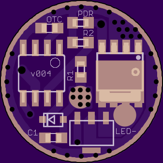
I am working on this board, do you have any advice to improve it?
https://oshpark.com/shared_projects/jZxjYbXN
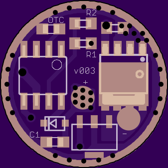
I recommend that you avoid placing vias directly on pads. Other people have already learned that the hard way.
Best practices also dictate not putting vias under components at all, but that’s just to make the circuit easier to read visually.
I have not looked closely at the layout. One thing which you may want to consider is how much of a pain it is for someone to do the Zener mod.
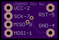
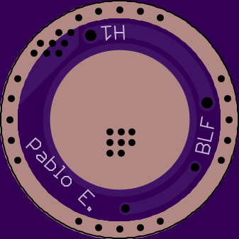
You all know where this is going  . You can use this to program the tiny attiny25/45/85 MU MCUs. As usual, the spacing and via sizes are suitable for standard header pins. Like the other board, I have labeled the USBASP pins for easier hookup (I'm not the only one to ever mix those pins up, am I?
  )
)
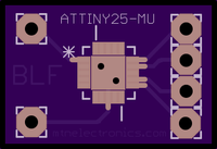
As usual, I have already tested it and it works.
Every one has their own design choices, but given the choice I also never like to have exposed pads directly against the ground ring because the solder always goes there, and often can pull the component in that direction as well.
When designing a circuit, it is always important not to think not only about the circuit functionality, but about ease of assembly and installation. Often, due to space constraints, we have to sacrifice a little bit to make things fit, but it is always important to keep the end goal in mind (actually building the driver and being able to use it in a flashlight).
Sorry for the question but how does this aid in programming the MCU's?
Well, I spent hours trying to get my programming clip on one of those MCUs and it didn't work, so I called up Dale and he told me to put the clip in some liquid nitrogen to try and shrink it down a bit. Next, I e-mailed Steve who machined me a beautiful polished aluminum adapter to try and program the chip, but that effort also proved to be futile.  Just joking.
This is for the smaller leadless package of the attiny25/45/85 MCUs. You can't program them with a clip, and commercially available programming devices are fairly expensive, so this is an easy alternative. You could also put breakout pads/pins on the driver and solder wires to them to program on a driver, but I find it easier to program them beforehand and save the space--since saving space is the only reason I would ever use one of these MCUs.
Thanks both of you for the advices, and welcome back to the forum wight.
@wight
I didn’t know vias may cause problems, i have seen them on pads sometimes and i had assumed that it was ok.
Better to learn it the easy way :bigsmile:
Right, i have overlooked zener mod, i will see what can be done.
@RMM
Can a component be pulled throught those tiny corners? :~
Anyway that can be solved easily, exposed ground ring is 0.75mm width, so i can shrink it to 0.5mm.
Sure, installation and ease of assenbly will be tested in nexts steps.
Thanks RMM. I asume they only have four legs? I have components on order to program the Attiny MCU's hopefully with the help of a very patient member her, I hope. Lets hope its not to late to teach an old Moose new tricks.
No, these ones have 20 pins, but only 8 that are actually used. Start with the regular SOIC-8 MCUs.
I think it just looks that way in the oshpark renders. In their render it enlarges the pads to the point of overlapping, looking like one (or 4) big pads instead of a bunch of tiny ones.
Wow, 20 pins. It will be an achievement for me to do anything with the 8 pin. I'm starting with the 7135 based drivers.
If i understand well how zener mod is done (i am a bit confused with post of different dates, where capacitor is placed before or after diode) i don’t have to tweak anything, zener can be placed just over left side of D1 and C1.
Just a stroke of luck, I designed the board this way, keeping in mind being able to place a C2 for 25/45/85 MCUs.
Aha, I knew something must have changed while I was gone! New tricks!
To better illustrate, here’s a different illustration of RMM’s adapter:

I haven’t used the adapter of course, but I assume that for optimal use solder is lightly wiped across the adapter and allowed to cool. Then one simply presses the MCU against the PCB where it would normally be soldered on. Once you’ve got it in place and held down you can program it normally. Someone may correct me here though. (?)
I am not sure that I understand everything you said. The Zener mod is very simple, but due to my time away I had to think about it / double check a bit. The Zener mod requires two additional components: a low-value resistor (such as 200 ohm) and an appropriate zener (such as MMSZ5229B for example). The resistor should be placed between MCU Vcc and Vbat. The Zener should also be attached to MCU Vcc - it will pull the voltage down to the appropriate level. Without the resistor in place the Zener will burn up. See comfychair’s post #9 here using the userscript I posted in my post #104 here for a semi-illustrated semi-guide to the Zener mod.
Unless I am mistaken, this means that for a Zener build a person would replace D1 with the 200 ohm resistor, then place a Zener between the lefthand pad of the resistor and the lefthand pad of C1. I think that this will be a pain as you have things setup now: trying to set a 0603 or 0805 component on those little diode pads will result in the component wanting to walk/spin… probably getting stuck to C1 sometimes. Stacking the Zener on top will probably also be a bit of a pain.
Everything RMM brings up here is important and worthwhile to think about. I personally also try to keep my component pads out of my GND ring. As you can see by looking at my drivers, I frequently fail. (a) the components can be pulled toward the ground ring (b) the GND ring can get unwanted solder wicked onto it. Mostly (a) is the big problem IMO: sometimes clearances demand that components stay far away from the edge of the flashlight, not skew on their pads towards the outside. Surface tension with solder is surprisingly strong sometimes and will pull a component right off of it’s pads. 7135’s and FETs are notorious for this, which is why I was very careful to implement a small “dam” of resist on drivers like the A17PZL. Without this the 7135’s will pull all the way to the edge of the GND ring. 2-pad passives are not as bad, but it’s still an issue.
You have the main FET current traces taking up all available space. Why not make all traces, even low current ones, on both sides, as wide as there is room for? That would add a little more to the heat transfer, and maybe the capacitance between sides of the board would protect a little against high frequency switching transients.
Thanks wight. I now understand the MCU sits in the middle hence the 20 pins. I was looking at the four on the outside edge.
I measure a diameter of the GND-copper that is always 0.6mm smaller than the board. Got 3 very recent boards here (all ordered last November):
22mm board, 21.4mm copper
17.4mm board (I’m long since overshooting and filing down…), 16.8mm copper.
15.4mm board, 14.8mm copper.
It’s already difficult to solder the boards to some pills. With this added 0.3mm all around it’s nigh impossible.
Thus the workaround.
The 0.8mm PCB is a great option, by the way.
HQ
Thanks HarleyQuin. My measurement of ~0.2mm was for only one edge. I did not measure the overall dimensions of any of the drivers. Still, I think the smallest feeler gauge in my set was 0.25mm and the missing material was less than that much for me. In any case our measurements are pretty similar: ~0.4mm overall and ~0.6mm overall.
Thanks, now is perfectly clear.
That is what i think, but i had found this thread with C1 between resitor and gnd, and i knew that this cap position is something from the past on 1S configurations, but i didn’t know if it still was doing like that for zener mod.
You are completly right, i was so concentrated on finding where to place zener, that i didn’t realize that resistor would have to be soldered on those tiny pads.
That is someting you can take for granted i do, i just was surprised.
I have narrowed exposed GND ring to 0.5mm, i hope it is enough.
I am still working on zener mod capability, but here are the changes I’ve done for the moment:
-Wider traces
-Some components relocated (far from vias)
-Narrower exposed GND ring
Thanks all for the sugestion, if there is someting more you think could be improved, let me know.
Has anyone laid out an 8mm XM-L, MCPCB?
If not, who can?
Thanks!
The problem is that custom MCPCBs (metal core PCBs) are quite expensive. Do you have a source with a decent price?