You have the main FET current traces taking up all available space. Why not make all traces, even low current ones, on both sides, as wide as there is room for? That would add a little more to the heat transfer, and maybe the capacitance between sides of the board would protect a little against high frequency switching transients.
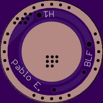
Thanks wight. I now understand the MCU sits in the middle hence the 20 pins. I was looking at the four on the outside edge.
I measure a diameter of the GND-copper that is always 0.6mm smaller than the board. Got 3 very recent boards here (all ordered last November):
22mm board, 21.4mm copper
17.4mm board (I’m long since overshooting and filing down…), 16.8mm copper.
15.4mm board, 14.8mm copper.
It’s already difficult to solder the boards to some pills. With this added 0.3mm all around it’s nigh impossible.
Thus the workaround.
The 0.8mm PCB is a great option, by the way.
HQ
Thanks HarleyQuin. My measurement of ~0.2mm was for only one edge. I did not measure the overall dimensions of any of the drivers. Still, I think the smallest feeler gauge in my set was 0.25mm and the missing material was less than that much for me. In any case our measurements are pretty similar: ~0.4mm overall and ~0.6mm overall.
Thanks, now is perfectly clear.
That is what i think, but i had found this thread with C1 between resitor and gnd, and i knew that this cap position is something from the past on 1S configurations, but i didn’t know if it still was doing like that for zener mod.
You are completly right, i was so concentrated on finding where to place zener, that i didn’t realize that resistor would have to be soldered on those tiny pads.
That is someting you can take for granted i do, i just was surprised.
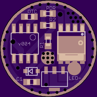
I have narrowed exposed GND ring to 0.5mm, i hope it is enough.
I am still working on zener mod capability, but here are the changes I’ve done for the moment:
-Wider traces
-Some components relocated (far from vias)
-Narrower exposed GND ring
Thanks all for the sugestion, if there is someting more you think could be improved, let me know.
Has anyone laid out an 8mm XM-L, MCPCB?
If not, who can?
Thanks!
The problem is that custom MCPCBs (metal core PCBs) are quite expensive. Do you have a source with a decent price?
I wish.
Starting price 30$ for 10pcs 5x5cm.
OH!!!
Wonder if gerbers sent to them, the pad under the heat slug could be left open and auto filled with HASL from the factory ![]()
Awesome! Thanks.
I don’t think it’s likely that they will be setup to do that. We also don’t know at what point the fiberglass (dielectric) layer is bonded to the metal core.
No harm in asking though. Worst they can do is say no.
If you make this too narrow and don’t make your PCB larger than 17mm diameter you’ll find that the exposed area of GND ring will sometimes disappear during production. If you look carefully at some other drivers you’ll note that they are setup with a thin exposed GND ring plus larger exposed areas where possible.
The A17PZL is a good example actually. Take a look at the OP in that thread. Note that there are narrow GND rings on the top and the bottom. The primary ring on the bottom is skinnier than the ring on the top. The exposed part of one on the bottom completely disappears when OSH Park produces the board! Fortunately the bottom of that board has exposed scallops which are still there. You can see of of that in the 4 pics in the OP.
What you'll find is that if you are pushing the limits too much on copper thickness, trace thickness, drill hits, solder mask, etc., that you will often get boards that aren't 'as expected'. Oshpark uses several different fabs, so sometimes you can get a board and it will be different than other boards. The Chinese fabs seem to be even more fond of making arbitrary changes, so be careful.
Can anyone here convert an autocad to gerber for the place listed above?
PM me if you can. Thanks!
Autocad is not for pcb design.
So there is not going to be any automated way to convert autocad to gerber.
Let me rephrase it then. Can someone recreate the autocad into a gerber?
Did you post your DXF/whatever somewhere? A straightforward conversion would be to export bitmaps and then use Eagle or KiCad to import the bitmaps into layers. From there you can export a set of gerbers.
This process can generate rough edges. In the past for my own purposes I’ve exported high resolution bitmaps at 4x my desired size. I would then import them into KiCad and save that. At that point I’d use a web service to reduce them to 25%. (the web service is intended to help fix stuff like putting logos on silkscreen art). Once they were reduced they were the correct size of course and I’d reopen the files in KiCad and export gerbers. It’s a lengthy process because you must do it for every layer. Good luck!
I got a batch of boards with empty ring on the edge, but i thought it was a fault because the LED+ was not exposed and in the second batch were copper to the edge.

Seeing the second board i didn’t know why OSHpark recommends at least 15 mil (0.4mm) clearances from traces to the edge of the board, but now i know there are variation between different fabs, it makes sense .
Great tip, i’ll put into practice.