The problem is that custom MCPCBs (metal core PCBs) are quite expensive. Do you have a source with a decent price?
I wish.
Starting price 30$ for 10pcs 5x5cm.
OH!!!
Wonder if gerbers sent to them, the pad under the heat slug could be left open and auto filled with HASL from the factory ![]()
Awesome! Thanks.
I don’t think it’s likely that they will be setup to do that. We also don’t know at what point the fiberglass (dielectric) layer is bonded to the metal core.
No harm in asking though. Worst they can do is say no.
If you make this too narrow and don’t make your PCB larger than 17mm diameter you’ll find that the exposed area of GND ring will sometimes disappear during production. If you look carefully at some other drivers you’ll note that they are setup with a thin exposed GND ring plus larger exposed areas where possible.
The A17PZL is a good example actually. Take a look at the OP in that thread. Note that there are narrow GND rings on the top and the bottom. The primary ring on the bottom is skinnier than the ring on the top. The exposed part of one on the bottom completely disappears when OSH Park produces the board! Fortunately the bottom of that board has exposed scallops which are still there. You can see of of that in the 4 pics in the OP.
What you'll find is that if you are pushing the limits too much on copper thickness, trace thickness, drill hits, solder mask, etc., that you will often get boards that aren't 'as expected'. Oshpark uses several different fabs, so sometimes you can get a board and it will be different than other boards. The Chinese fabs seem to be even more fond of making arbitrary changes, so be careful.
Can anyone here convert an autocad to gerber for the place listed above?
PM me if you can. Thanks!
Autocad is not for pcb design.
So there is not going to be any automated way to convert autocad to gerber.
Let me rephrase it then. Can someone recreate the autocad into a gerber?
Did you post your DXF/whatever somewhere? A straightforward conversion would be to export bitmaps and then use Eagle or KiCad to import the bitmaps into layers. From there you can export a set of gerbers.
This process can generate rough edges. In the past for my own purposes I’ve exported high resolution bitmaps at 4x my desired size. I would then import them into KiCad and save that. At that point I’d use a web service to reduce them to 25%. (the web service is intended to help fix stuff like putting logos on silkscreen art). Once they were reduced they were the correct size of course and I’d reopen the files in KiCad and export gerbers. It’s a lengthy process because you must do it for every layer. Good luck!
I got a batch of boards with empty ring on the edge, but i thought it was a fault because the LED+ was not exposed and in the second batch were copper to the edge.

Seeing the second board i didn’t know why OSHpark recommends at least 15 mil (0.4mm) clearances from traces to the edge of the board, but now i know there are variation between different fabs, it makes sense .
Great tip, i’ll put into practice.
Yeah, that kind of change is a bummer. I have about 500 17mm boards with no exposed copper behind the FET. Same exact file I had already ordered dozens of times, but the time I went to order the most look what happened!
If you look at the silkscreen and milling/drill hits you can often tell which Oshpark fab they were from. I can distinctly tell the differences between them, but you never know which one you're going to get.
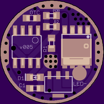
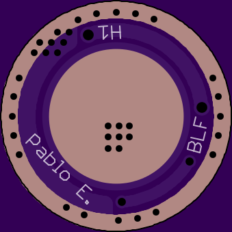
It has been a lot of time since i posted v004 (I have been a bit busy due to exams), but today i’ve finished a new version.
Theese are the changes from v004:
–0603 diode pads (for zener mod)
-More exposed copper on top GND ring
-Added copper pour under MCU for temp sensoring
-Wider bottom GND ring near FET vias
https://oshpark.com/shared_projects/tjm3DzQH
As always, any suggestion will be welcome.
Nice, one question is it “only” a design change to wights A17DD-L or is there any extra functionality?
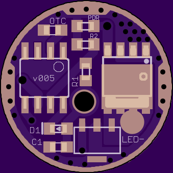
Is it possible to drill through that LED+ pad and push a cable through? Could you already make a hole there? This way you can use the same cable to bypass the spring and to get to the LED.
Hi finges,
there is an extra funcionaltiy, pads for a pull down resistor (PDR) to avoid "turbo to moon" blink.
I doubt a hole could be drilled, but i can make it in the design.
Stay tuned.
This version has been replaced by v006: Oshpark Projects - #1686 by Pablo_E
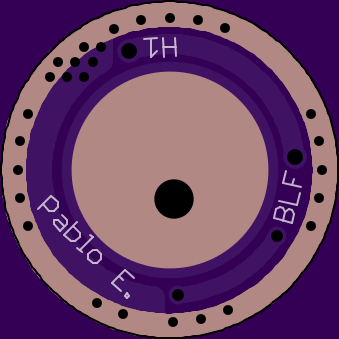
Done!
Hole (actually is a via) is 2mm/0.0787inch in diameter.
https://oshpark.com/shared_projects/rVrw8a4J
Very nice Pablo! Thank you very much for sharing. Only thing I’d like to see changed is the 0603 cap, I would prefer 0805 for an OTC.