Hi finges,
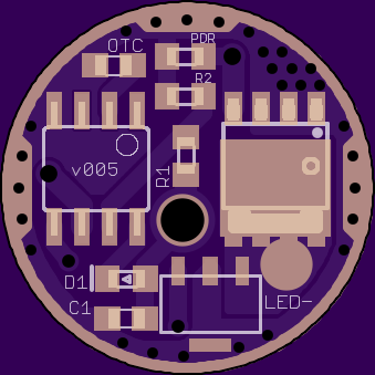
there is an extra funcionaltiy, pads for a pull down resistor (PDR) to avoid "turbo to moon" blink.
I doubt a hole could be drilled, but i can make it in the design.
Stay tuned.
Hi finges,
there is an extra funcionaltiy, pads for a pull down resistor (PDR) to avoid "turbo to moon" blink.
I doubt a hole could be drilled, but i can make it in the design.
Stay tuned.
This version has been replaced by v006: Oshpark Projects - #1686 by Pablo_E
Done!
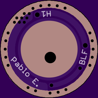
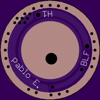
Hole (actually is a via) is 2mm/0.0787inch in diameter.
https://oshpark.com/shared_projects/rVrw8a4J
Very nice Pablo! Thank you very much for sharing. Only thing I’d like to see changed is the 0603 cap, I would prefer 0805 for an OTC.
+1
I think if you moved the FET pull-down resistor to right above the FET, you would have room for 0805 pads right at the top of the board.
Or rotate R1 90 degrees, then you can fit all three resistors side by side closer to the center, leaving plenty of room for a 0805 OTC pad.
But myself, I wouldn’t bother. I use 0603 on all my boards.
Don’t you consider soldering a 0805 cap on the 0603 pads?, I don´t know how difficult it is, but it fits (like in the right diagram)

Do you prefer the 0805 option?, if so it could be done performing both of your suggestion, i see some potential clearance problems but i think they could be solved.
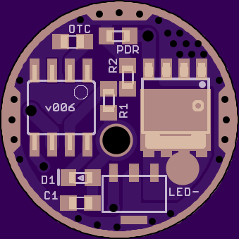
Yet another untested monstrosity… This implements what is intended to be a snubber for 1s applications, plus a bleeder for pilotdog68’s tailcap LED system, plus an OTC pulldown, plus a gate pulldown, plus a 3mm via for the BAT+ wire. There was no space for a BAT+ pad on top, so it’s bypass or go home. At first I thought that I was going to be forced to increase my normal 1mm physical keepout, but somehow I got away with it.
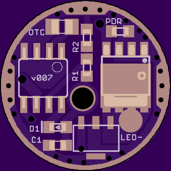
This version has been replaced by v007: Oshpark Projects - #1686 by Pablo_E
This board is really dense populated! you made a great job!
I have already changed OTC pads size to 0805, i have had to remove some vias, and voltage resistors may not be easy accesible, placed that way between tall components, but i think it is done.
https://oshpark.com/shared_projects/0NAo2EmQ
Thanks. ![]()
Your board is clearly improving, but here are a few things (in no particular order):
Thank you too! it is improving thanks to all of your help.
I going to reply in the same order:

where did you get your clip Pablo?
Is a chinese no branded one you can find on ebay, aliexpress and many other sites.
I got it from this seller: Henny Liu’s store , but i don’t recommend him/her as i got different clip from which is shown on advert images, so random version could be sent.
Here is a pic of the clip i have:

After a long exams season, i have found some time to work with eagle.
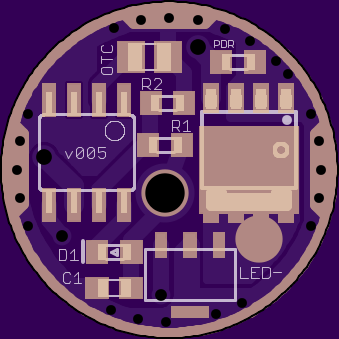
I have tweaked my two last designs, so people who want to stay with 0603 OTC could use v006.
Changes are:
- silk lines are now thicker
- R2 is not next to MCU legs
- versioning is again with numbers only.
I hope they are close to final design ![]()
The D01 contact board fell of the list and I have sold all of my spares… May be some small demand for it…
I need some help. So far everything I’ve done has had a perfectly circular milling layer. How do I do other shapes accurately? Like an SRK driver with the tabs, or a tailboard in the SRK “flower” shape or for a ZY-T08?
Hey… I am really stuck on the same issue!
Draw your basic outline, then use the split, miter, and meander tools.
Easy for you to say Richard! But this comes from a guy that build a D01 contact board and could not make a basic FET driver fit on board… I really suck at that program.
I’ve never touched any of those tools… I’ll have to play around with them and see what happens.
Thanks for the tip. Now that you know somewhat of the extent of my inexperience, feel free to keep the tips coming ![]()
For tabs I make them first and use arc to get the rest of the circle.