Oooohh! Another comeback of a BLF-legend! Comfy, thanks for all your great contributions in the past. Welcome back.
Oh, I see now that it is possible… you’re planning for Vcc to stay above B+, but only by a controlled amount that doesn’t zap the MCU. Is there anything to gain from that though? Have there been any problems caused by the swing in Vcc? I’ve been AWOL too long, I don’t know any of the new firmwares or the DD+7135 drivers.
Hey man, I’m just a blind squirrel who occasionally finds a lucky acorn. ![]()
- I’m fairly confident that I can get Vcc flatter than B+.
- Component location does matter. Remember, traces have inductance and resistance. It may not matter very much, but it matters. That’s not the central focus here and FWIW I use the term ‘move’ interchangeably for “logically moved in the circuit” and “physically moved in the layout”. I know, that should be a crime.
 In this case C1 has been logically moved to a different location in the circuit!
 - I don’t feel like building one either. :-/ I’ve got a nice scope which I picked up a couple of months after you did all of that work in your FETs and gate resistors - scope images thread. It was clearly a really valuable tool and I’d wanted to get on the oscilloscope bandwagon for a while. If I get one built I can put the scope on it and see what’s happening.
- Thanks for bringing up the capacitor in parallel to C1 thing… I completely forgot about it. AC / psuedo-AC is a mystery to me. I’ll have to think on that a bit.
EDIT:
Exactly! Yes, some members are using ATtiny25/45/84 and those seem to be more sensitive to a poor quality Vcc.
The new layout also makes this board “Zener mod ready” which it was not previously (doing a Zener build on v009 was at least a minor pain AFAIK). That said… I think it also means that a zero-ohm jumper should be used in place of the Zener’s load resistor when the driver is built for 1s use.
I know little to nothing about all these things, but I think this comment (#581) from Tom E in the attiny25 thread could be related.
EDIT: sorry, didn’t see the above two posts, this want meant as a reply to comfy’s post #331.
@Comfy, you seem to find very important acorns for a blind squirrel. ![]()
I dunno, the current through the Zener with 1S would depend on how much current the boost circuit is able to generate. I have no idea how to figure out what that would be except by poking it with a pointed stick. Since the boosting happens every time the output switches the amount depends on the duty cycle which changes with each mode/level. It would also change by battery type and also state-of-charge. Makes my brain hurt, easier to just build it and measure. I can only model it by comparing to a positive displacement pump connected to a variable speed motor…
On some high-powered FET lights, VCC spikes were rebooting the MCU. This happened sometimes as low as 5 amps, or sometimes required more like 12 or 15 amps to trigger. It was worst on strobe modes.
The short-term solution was to make C1 a lot bigger, but this design attempts to fix it more properly.
MCU can’t get a voltage spike on drivers where C1 has been relocated, Vcc tracks with battery voltage. That means B+ would have to bounce up over 6V when the output turns off, and I’d have to see a scope image of that happening before I would believe it.
I have no scope and virtually no clue about circuit design. I just know that some sort of spike happened at the trailing edge of a full-power pulse, when the FET closed, and the spike was enough to reboot the MCU. And, unfortunately, I got one of my drivers permanently stuck in 128kHz mode when I slowed it down enough to see what was happening.
(can be recovered with a high-voltage serial programmer or fuse-resetter, but I don’t have one)
I’d imagine that abruptly going from ~10 amps to zero hits hard enough to have a splash effect, but I don’t really know any details of what that effect would be. Any thoughts?
There’s a little bounce higher than resting voltage after the output turns off, but it’s small and very short lived. Pics in the scope images thread show a max of about 4.4ishV with a cell at 4V resting.
I have a 6x XML2 SRK, with the original BLF driver, without the giant capacitor or giant flyback diode or the choke/inductor. It’s an exact copy of the original 105C circuit with the exception of the 10uF C1 cap moved from after the diode to before the diode. It only gets used with 25Rs and I don’t have anything capable of measuring that kind of current but I would guess, based on output, it’s got to be near 20 amps. It doesn’t have any issues at all. I can’t think of a more extreme scenario than that one.
TK, are you sure this is happening with drivers with a revised PCB, one that does not use the original Nanjg diode/cap arrangement? Cause this sounds exactly like the problem I was fighting and solved with the relocated capacitor.
Yes, it happens on wight’s FET+1 drivers (this thread) (as built by either DB Custom or Manker), and on RMM’s FET+1 drivers. But it doesn’t happen on tiny13a MCUs — only on tiny25/45/85. Swap a tiny13a onto the exact same board and the rebooting stops. Or drain a cell 0.2V first and it works fine. Or use a low-amp cell. In some cases, it also depends on the quality of the springs connected to the battery, or even how far an individual spring is stretched or compressed. I could probably send you an affected driver if you want to look more closely. I don’t recall exactly where they all are right now (and most of them are bricked due to failed flashing), but I could probably find one.
The bricked ones are likely recoverable if I remove the MCU or perhaps some other component, but I haven’t investigated that yet. I just know that, for some reason, I can’t get Manker’s recent drivers to flash on-board. Other people have done it without issues though.
If the driver layout will allow it, rigging a second 10uF cap between MCU pin#8 & GND should prevent Vcc from seeing any of the battery voltage ripple. Check the two pics in the post I linked wight to above. Just for experimentation. That may not be the solution wight chooses, but it will definitely give you a 100% stable Vcc.
I think the cap between pins was something Tom E already tried, and it worked, and it worked with a smaller cap. I’m not entirely sure it’s the same as what you described though.
Hmmm, good point comfy. Maybe I’m over-thinking this.
Yeah but, the Zener regulator solution ticks more boxes than just ‘smooths Vcc’. It also makes several different types of driver possible using the same PCB. If it were a single-cell-only thing then I guess it would be a wash, even down to the same part count between them (assuming the single cell Zener version didn’t need a load resistor).
And, I have no idea what effect different values for the second cap might have. Tom I think used a 0.1uF in the original C1 location between pin#8 & GND, but there’s no scope images or other data to say what Vcc looked like. I only have that one pic using two 10uFs.
Yes - I've been using a 0.1 uF cap across the MCU, pins #4 to pin #8. On all the 85 board I've built on this wight FET+1 driver (v009, done maybe a dozen or so), this small cap does the trick - keeps the MCU running stable. I also use a 12K resistor on the SIR800DP (grnd to gate) when needed - that clears up the flash/blink on starting moon mode.
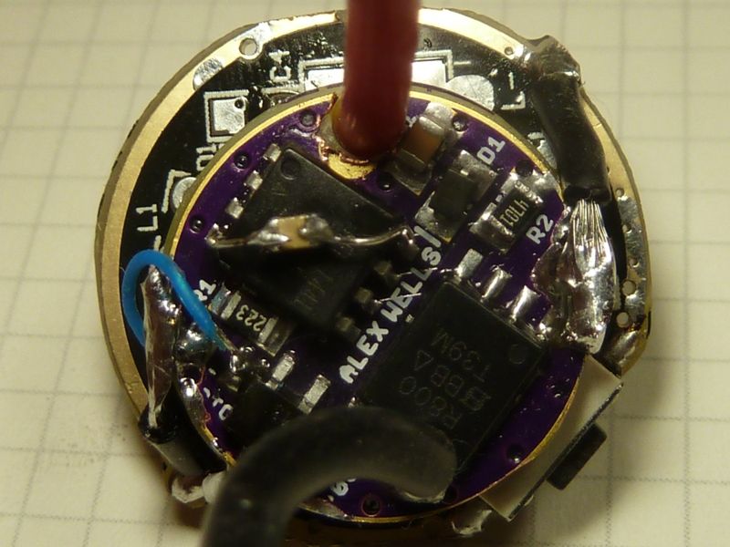
hers' an example showing the extea 0.1 uF cap wired (pic came out dark, sorry):
Thanks to you all for constantly fine tuning these drivers. Comfychair, welcome back!
.
As it is talked about re-moving (or adding) C1 behind the diode, I’d like to add some thoughts. Following some recent discussion I came to the conclusion that this might not all be common ground:
- The value of C1 - if behind the diode - influences OTC timing and the values needed for the CapThreshold in the firmware
- The stock value for C1 is/was not 10y, but 4.7y on a Nanjg105c(8x) and 2.2y on an AK47a(3x)
- Even the good X7R 1y OTC variates within the 20% spec and I measure between 0.83y and 1.07y
Note: All said is experience with linear driver (7135 only) where LVP is behind the diode and dual OTC threshold (3 timeframes) used.
When I started selfbuilding (linear) driver I used 10y for C1 as everyone else did, in the same time I used the AK47a as a single sided driver with added OTC. The OTC timing was greatly different (and I had to use firmware-values over 250 in some cases).
Then I started measuring the C1 stock values, as they were probably the basis for JohnnyC’s Star firmware. Of about 15 105c and Qlites I salvaged in 2014 all had a 4.7y C1 (may change or have changed with time and supplier). The AK47a on the other hand had a 0603 2.2y C1 - and I used some 10y. Results varied greatly.
So the value of C1 behind the diode does seem to influence the OTC timing.
The 20% production variance of the OTC influences the timing as well, but not as strong.
My conclusion was to bin C1 and OTC. I use C1 only in the range of 4.32y - 4.52 y and OTC in the range of 0.87y - 0.93y (greatest yield after binning…) and adapted my firmware to the middle values. I get very consistent OTC timing for dual threshold ever since.
This led me to the conclusion that the variance in the 1.1V voltage reference of the ATtiny13a a is negligible (a member had stated so somewhere).
I never followed the change to bypass the diode for LVP (R1 on Bat+) as this seemed to influence OTC timing as well. I had no intention to open that can of worms.
I just wanted to bring to notice, that if you re-introduce a cap behind the diode for FET-related reasons, that this might mix up OTC timing again as well. Especially if inconsistent values for C1 are used.
I never seen 'y' used for µF. Is this intentional?
For the example above in post #347, and I think for all my uses, using the 0.1 µF cap is for e-switch lights only, so these don't have a need for OTC (thank goodness!). Timing is rock solid, dead-on in the 85's for e-switch use, and long clicks are with the MCU running, so very different, much much better for the user experience.
It's a good point you are making though, since the vast majority are still modding clicky lights, and I and others see timing issues with the long clicks for OTC.
I had not heard about 4.7 µF caps used in 105c's and Qlites. Maybe the 10 µF was measured earlier than 2014? It's easy to measure a cap - I've done it several times, but don't recall someone actually measuring the values.