Attiny25/45/85 FW Development Thread

I think this tread should be made sticky, I think lot of people (building FET drivers) have missed this

BTW, from my own research gate and gate pulldown resistors increase inefficiency of the FET by increasing time required to turn it on. Only after FET has been turned on, it has low resistance&heat disipation.

In the solution from the above thread, only a new 10uC cap across +Batt and GND was needed. I think the old Cap & gate resistors are to be removed. Check it out, very interesting thread.

The gate pull down resistor is a good thing normally, a FET gate should not be left ‘flapping in the wind’. One of those components left out for simplicity and PCB size limitations. It may help for the flash some get when going from full-on to moon mode or similar.

True, but the idea is just to take the edge off, not to dampen it so much that the FET is operated any significant time in the linear region. It does put a limit on maximum sensible PWM frequency to use. See the recent BLF D80 driver for an example of how not to do it.

These things are like the suspension on a car. Too hard, or too soft, and you are bound to have a bad time depending on the road you are trying to follow.

EDIT: Thank you for that thread link, but probably the thread discussion was around tiny13a drivers? Seems the 13a is much more forgiving than the bigger MCUs. Local decoupling on any chip like an MCU is basic stuff, it should not be neglected like it has been.

K, spent some time reading thru the comfy FET scope images thread. Post #44 seems to be the result (??) - 10 uF cap in parallel with the diode. I gotta try this... This is old stuff - I followed the thread at the time, somewhat. With all the pics back, it's once again useful info.

Dunno.... Really not sure if I can understand it all, and if there is a final solution from it. dave_'s posts seem impressive/correct, but no real solution posted as a result?

Just fyi, the 10K-12K 0805 resistor I use on the FET gate (to grnd) always works!! No loss of output, definitely gets rid of the flicker switching to moon mode. I've experienced those flicker problems in lights, tore them apart - added the resistor, and then flicker is gone!

Update: removed the 0402 10K resistor, put a 0805 12K in it's place, and with the stacked 10 uF cap, the mode changing problems all seem to have gone away! Dont have any other caps or other extra resistors, just the two 10 uf caps on C1. Testing was on the bench - installing it now in the JM70 light.

I have some of these 22uF Caps ready to try, rather than stacking the 10’s, but don’t currently have a driver that is playing up to test one out.

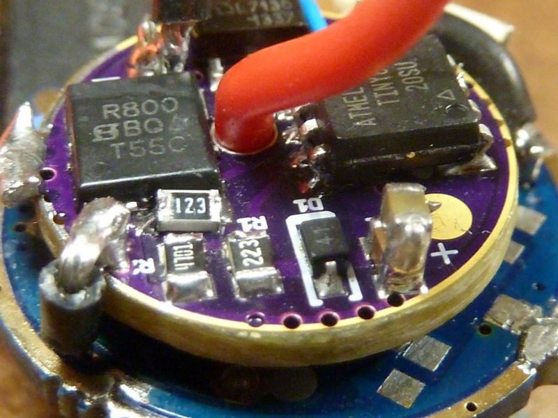
Regarding the inductive ringing at the off edge of the PWM or strobe pulses, this is what we are dealing with:

Yellow trace is the voltage at the drain of the FET (so 0 V = FET full on, 0 V is at the second division from the bottom).
Blue trace is the voltage at pin 8 of the MCU, same scale.
This an A6 driver from Banggood driving one XM-L2, using a fresh 30Q cell.

We can see some boosting of the pin 8 voltage.
Note the FET drain peaks at > 6 V at switch-off.
Also note the frequency of the oscillation, around 10 MHz. We’re in HF radio frequency band.

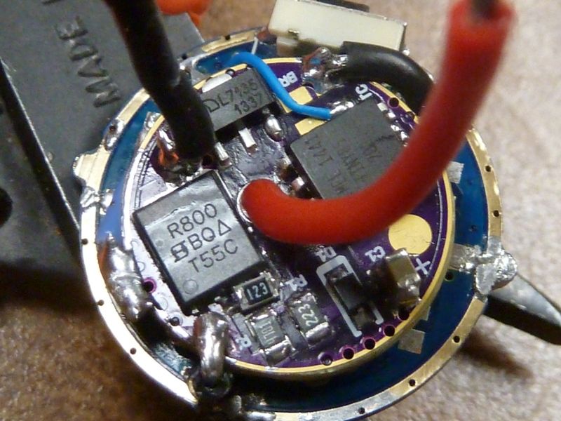
Now lets shorten the wires between the emitter and the driver from 4” to 1”:

Frequency of the oscillation goes up, but peak goes down below 4 V - as can be expected with the lower inductance of the shorter wiring.
I know adding a gate resistor will tame that oscillation, but I did not want to scrap the driver (yet), so tried a drain-source snubber on the FET:

The snubber consists of a 0.1 uF capacitor in series with a 4.7 ohm resistor. Not calculated and for sure not optimum values, but a good improvement.
Something you might want to try Tom, if all else fails. For the test I used regular TH components with the leads cut short. One leg of the snubber capacitor on the black wire pad, one leg of the snubber resistor on the tab of the 7135 (better option would be the source pins of the FET).

The voltage at pin 8 of the MCU looked surprisingly good, all things considered. I would not use more than 0.1 uF between pins 4 and 8.

Emitter wire length also makes a big difference, so keep them short. This is also with the snubber, but with the 4” emitter wires:

The assembled light is working pretty well, as described earlier: 85, 2 uF caps in parallel on C1,12K FET gate resistor to ground.
The ThorFire JM07 hits 1900 lumens at start with an XM-L2 U4 1C, 56 kcd, UCLp lens, spring bypass’s, on a BASEN IMR 4500 26650. Running Narsil of course, but not sure yet if everything is ok - seems the clicky switch is not working for mode changing, though it seemed to work fine on the bench — no OTC cap, but seemed to work on other builds even without enabling brown-out in the fuses. Also memory seems to be turning on, even though it’s turned off - not sure if this is a straight bug or not, but never seen this before.

What you have there looks good - got to study this more. Hhmm, don’t even have the 0.1 uF cap across pins 4 and 8 now…

You just answered months worth of questions, speculation, and argument. Seriously, this is extremely helpful information.

Also, I didn’t realize that my long emitter wires were making the problem worse. Oops. I just thought it might reduce overall output by a tiny bit while providing much easier access for flashing; didn’t realize it would actually worsen the voltage spike.

A while ago I managed to figure out that the worst spike was on the trailing edge of a FET pulse, by slowing a driver down so far that I could see the individual pulses… but I, um, didn’t realize that would also make the driver un-flashable without special hardware. Oops. I should probably get myself a fuse resetter or high-voltage serial programmer.

Anyway, your tests just now settled quite a few open questions and the scope images make it much easier to understand. :slight_smile:

Looked this over more carefully. There's a lot to this I'm either learning, or not quite understanding - I don't have a good electronics foundation, but Wikipedia has just helped me out a little (now I know the "drain" of a FET is the output).

The length of the LED wires, and the location of the snubber is a surprise to me - in my limited knowledge, once the signal goes out the FET, you are done - why would it have any effect at this point? But apparently it does.

The other thing I don't understand was I thought our main concern is the MCU pin 8 input - spikes, voltage boosts causing MCU resets and strange behavior, etc. But in the scope images, it looks like the blue trace is pretty much unaffected?? So, I don't understand, but I'm guessing the problems I'm seeing are more about the FET and not the MCU?

In this particular light, and all I work on, I keep the LED wires at their minimum. Only lights they have to be long in are SRK or multi-LED types that have a screwed down reflector, so you have to have extra lengths of wire to keep the driver dangling when screwing down the reflector from inside the pill area.

TK, happy to help! :slight_smile:

Tom, pin 8 is important. Every time we switch the FET on we basically short pin 6 to ground (momentarily, while the FET gate charges up), This current is limited by the output impedance of the pin 6, but probably peaks at around ~50 mA. This current has to come from somewhere, and somewhere very close by, otherwise the voltage at pin 8 will dip. Enter the local decoupling capacitor. Which we do not have in the current design.

But, as you say, pin 8 looks surprisingly good under the circumstances, for the 13A anyway… And the corruption mechanism seems to be over-voltage, not under-voltage.
There is also the possibility of EM interference. AC currents tend to induce currents in neighboring conductors, look at that 10 MHz oscillation.

Can you try the snubber on a light that is troublesome?
Exact values are not important. Optimum values will depend greatly on the exact layout, wire lengths, etc.
Try a C of 0.1 uF and R of 2.2 to 10 ohm.
This was my crude arrangement, leads should have been shorter on the snubber components:
(As mentioned above, a better arrangement would be to have the snubber span the FET. Easy to do with SMD parts, but I do not have big selection of values in SMD.)

OK, bent up the gate leg of the FET and wired in a gate resistor.

End result is better than with the snubber. Turn-on time is 5 times slower, 500 ns vs. 100 ns. So PWM faster than ~4 kHz will not turn the emitter on reliably at 1/255 PWM duty.

From yesterday, basic A6 driver, short emitter wires:
(Yellow = FET drain, Blue = MCU pin 8)

From yesterday, with RC snubber added across FET:

Now with Rgate = 100 ohm added, and snubber removed:
(Purple trace is the FET gate voltage.)

Turn-on without Rgate:

Turn-on with Rgate:
(Note time scale is 500 ns/div, compared to 100 ns/div above).

Sorry, should have added above, the top three scope shots are of the turn-off with various configurations.

EDIT: Photo of the crude test setup with the gate resistor in place:

Well, I have to create a trouble-some light at this point. I got my JM07's driver out now - I have the 12K resistor on the gate and dobled up C1 cap and it works fine.

Should I remove the extra cap and see if the problems come back? If so, then try it with leaving the 12K resistor on?

This is what it looks like:

Might be better starting with a clean driver. I got to reflow up a few more anyways... What do you think?

PWM will likely remain in the range of 9 kHz to 31 kHz (usually 15-19 kHz). However, it’s not required to have level 1/255 working; it’s a simple enough matter to use a higher floor. I can adjust the output calculation scripts and PWM levels without too much trouble.

Current FET designs actually light up at PWM=0/255 in “fast” mode at 16 kHz. That’s basically half a frame, or … (quick napkin-math estimate) probably around one eight-millionth of a second. Ish. It’s generally considered a harmless quirk, but fixing it would make some of the code a little easier.

In my 85 firmware, I stopped using PWM "fast" mode - only use PHASE mode now, but Phase mode is still quite fast, think in the 15-19 kHz range. I dunno if we want to return back down to 4 kHz or lower...

Yeah, phase-correct mode on tiny25/45/85 is pretty awesome. It runs at precisely 15.6 kHz with nearly zero variation between units, it has none of the side effects of “fast” PWM, it’s fast enough to be invisible during use, and only a tiny slice of the population can hear it.

The main downsides are that it’s not quite beyond human hearing range, and it requires running the MCU at 8 MHz instead of under-clocking for lower power. I’d prefer 10 MHz / 19.5 kHz instead, but that’s not really an option with current hardware.

The common nanjg 4.5 kHz PWM is both audible and visible during normal use. :frowning:

I’ve already done experiments on FET-driven moon modes with extra-fine pulse time adjustment. It didn’t work very well, and varied quite a bit with cell voltage even after voltage-adjusting the pulse timings as much as the attiny allows.

In contrast, a 7135 chip pretty much “just works” with no fancy algorithms. “Boring” can be a good thing.

If moon is the only non-FET mode desired, it’d probably work to simply replace the 7135 with a resistor and drive the LED directly from the attiny pin in moon mode. It would only work for moon mode though, not any of the other low/med modes in the 1 lm to 150 lm range. So, those would have to use the FET and would have their efficiency reduced.

I would suggest putting the driver back to stock and make sure it malfunctions. Keep in mind the ringing is much worse with a fresh hi-drain cell. Although not shown above, I did confirm this with different types and state-of-charge cells.
You can leave the 12 k though, it should not come into play.

Then you have two options.

The easier option is to add the snubber. Dead-bug style across the FET. This option does not affect the switching frequency, if you have any reserves about the PWM frequency limitations.

Second option is the gate resistor. Only one component to add, but more difficult. It is more efficient at lowering the turn-off spiking/ringing. Do not be too much concerned about the lower turn-on speed. For reference, with a 100 ohm resistor, my FET still switched about 15 times faster than a 7135. Of course you can always use a smaller resistor. Smaller resistor = faster FET, at the expense of more ringing.

How does one leave a FET gate drive floating? Since it must be 0-255, what value would be floating? Moon mode only uses the 7135, so the FET PWM output is set to 0, and typically the 7135 PWM output value I use for moon mode is 3. The MCU's have internal pull-downs on I/O pins as I understand it. These MCU's are quite advanced.

Section 10.1 of the Data Sheet on the 24/45/85 (http://www.atmel.com/images/atmel-2586-avr-8-bit-microcontroller-attiny25-attiny45-attiny85_datasheet.pdf) says:

All AVR ports have true Read-Modify-Write functionality when used as general digital I/O ports. This means that

the direction of one port pin can be changed without unintentionally changing the direction of any other pin with the

SBI and CBI instructions. The same applies when changing drive value (if configured as output) or enabling/disabling

of pull-up resistors (if configured as input). Each output buffer has symmetrical drive characteristics with

both high sink and source capability. The pin driver is strong enough to drive LED displays directly. All port pins

have individually selectable pull-up resistors with a supply-voltage invariant resistance. All I/O pins have protection

diodes to both VCC and Ground as indicated in Figure 10-1. Refer to “Electrical Characteristics” on page 161 for a complete list of parameters.