Try the two-10uF setup, one before & one after D1. That helps with the bounce at B, and also allows a tiny bit of boosting at Vcc (but with B flatter, the boosting is kept below critical levels).
Well, I built a v009 today to install into a light I need to get rid of… and sure enough I ran into the “bright flash” issue you’ve been talking about Tom E. I didn’t do any measurements - I just installed a 0803 12k resistor as a gate pulldown (as you suggested). Problem solved. Thanks!
Yes, it’s just an idea for potential future use. It might be nice to get rid of the need for the voltage divider, assuming the idea would work as intended. It would only work on 1-cell lights, and only on tiny25/45/85, but if those limitations are okay it might free up a little board space for other things.
Gotcha, just wanted to make sure we were on the same page.
(quoted a bit out of order ![]() ) Bad news! I think that v030 should be usable for myself / DB Custom / Tom E… but I did make a mistake and forget about it when those two asked whether the boards were usable. I forgot to hook the 7135 up to LED-.
) Bad news! I think that v030 should be usable for myself / DB Custom / Tom E… but I did make a mistake and forget about it when those two asked whether the boards were usable. I forgot to hook the 7135 up to LED-.
I reflashed my own built-up v030 board several times before the problem occurred to me. I just couldn’t get moon to light up at all…. of course not, it was on the 7135! I bridged the connection with a small piece of solid wire from a component lead and it works fine. The good news is that the stencils won’t change for v031, no pads have moved. ![]()
Here is v031: OSH Park ~
Other topic: I do plan to revamp the spring side again. The current spring pads don’t seem to be a good match for the springs I’ve got. I’m open to input on spring sizes! Scraping’s always an option, but I’d like to accommodate 2-3 common sizes. My initial thought is [Nanjg-105 size], [common medium springs like the gold plated ones from MTN/Intl-Outdoor & the cheap Phosphor Bronze ones from Simon/etc], [big size? Like the ones djozz had made?].
And R1/R2 are still labeled in reverse?
Crap, yes.
Thanks Sharpie!
- It could, but I’m trying to avoid stacking. (I definitely don’t see any space savings from setting them side by side.)
- Correct, I see in retrospect that I wasn’t clear - those were simply the parts I had available. Having so many wrong-size parts made it very difficult to assemble, but they were available and I didn’t have the right stuff. I didn’t purchase any new components for this build. My intention was to use something more common like 5.1v, although I was concerned once I saw how high the 4.3v Zener was able to spike. Maybe the load resistor will help - there wasn’t really enough physical space to install a load resistor in that build and test it out (due to the 0805 and SOD-123 stuff).
- Yes, I agree about parts of this suggestion. A fresh component footprint would help with locating the part while soldering, but that’s about it. Locating the part better while soldering is definitely worthwhile and a new footprint is on my list. The full footprint won’t help a bit with the rest, but that’s OK…
- I suspect that this PCB is quite a bit tighter than you may realize. Sorry that I have not posted pictures of the build and I’ve moved the only driver I built into a light now. Considering that the intention is to operate at high currents a small solder pad won’t really do the trick. My current recommendation for using a brass post is to drop your wire down and solder it onto the top of the brass post, exposed through the large 3mm via. I don’t see why this wouldn’t work fine. Since I also sometimes use brass posts I’ll try and give it a try. With that said, let’s put a pin in the topic of ’LED+ solder pad’ for the moment. If you’ll look at my other layouts you’ll see that I always strive to include good solder pads where possible. Unfortunately due to the nature of these tiny boards we just can’t have everything all at once. Once this board is tuned up maybe a different one will support a decent pad. Or maybe we’ll save enough space to do it here in the end. It’s at the bottom of the list for the moment though. 8-|
- Soldering the LED+ wire into a via is not the way to get the lowest resistance (that’s why we have a bypass hole!). A wire with 2mm jacket won’t fit in the suggested location and would block popular Pomona clip.
- I’m afraid that this will interfere with larger B+ springs. (Take a look at the Gerbers from OSH Park if you haven’t - you’ll see what I mean.) We can check measurements to confirm that, but for LED- wiring at least I don’t see an advantage to through-hole. As far as drilling out to isolate… I’ve often suggested a lot of scraping for various niche applications (or even some more common ones :
(lesson learned) - if there’s no good reason to add drilling I’ll do my best to avoid it.
- That’s a topic I’ve been trying to get a handle on. I’d love some insight into choosing the freewheeling diode. I read and understood your post about it needing to be located at the driver in order to operate properly (at all!), but as far as component selection I’m pretty far out at sea. Could you suggest some likely candidates and explain why they are good choices? Or link to some good reading material which isn’t too high-level?
RE:PS: That sounds interesting. I was planning on trying 100nF, but not because I understood what would make it better. ![]() Could you help me understand why reducing C1 from 1uF to 100nF would be beneficial?
Could you help me understand why reducing C1 from 1uF to 100nF would be beneficial?
As far as not shorting R3 - I agree. Personally my plan was to put a value of 10R in place and then measure voltage drop with the scope to get an idea of what was going on in terms of current. Clearly it’s going to be a really spiky…
RE:PPS: OK, sounds like a plan to me. Can you think of any disadvantage of increasing the values of the voltage divider by 10x or more? Frankly I’m currently focused on the other stuff and may not jump on that part right away. Hopefully some other members will start playing before I do.
I have solder paste masks and boards should be here tomorrow or the next day.
For sake of the argument, I re-built my Jax X6 Hunter tonight with a new MT-G2 on a 25mm MaxToch copper mcpcb. With brand new Basen 26650’s (came in today) it pulls 11.50A at the tail and makes a whopping 4571 lumens from the big die! And the hot spot is surprisingly tight, probably the tightest yet from an MT-G2 and I’ve got 12 now. (the BTU Shocker only counts as one, although it has triple 9V MT-G2 emitters, worthy of note due to it’s single A17DD-S08 Zener modified driver making 10,000 lumens. My other BTU Shocker uses a like driver to triple XHP-70’s for up to 20,000 lumens in one brief test. So yes, the large via for through board direct positive can be a HUGE deal!)
18 Ga Turnigy leads, I had to use extension tabs off the 25mm mcpcb to allow the reflector to sit flat down on the surface, this after having previously cut the reflector’s aperture square to encompass the big substrate.
Using an older 2 sided driver, big Vishay 07N02 FET piggybacked onto the original 22mm stripped driver board. Power, it’s all about Power!
Oh No! Went to check my order status for the v030's, and there was none - forgot to order them  . Good news is I can order the v031's, or should I wait on v032's?
Dale (off topic a bit) - how do you like the Basen cells? At first, I saw them beat the EFEST 4200's, but since then, measured in different lights and see the EFEST's beat'n the Basen's, but still head to head in 1-2 lights... It's all very confusing, then again, I'm only looking at tail amps via a clamp meter and not comparing @start and @30 secs lumens measurements, and we know slight amps differences don't mean the same for output.
Still love the Basen cells. My measured all 4500-4600 capacity at 1A discharge, but read someone else posted bout 4100 mAh tested.
Best cell I ever tested in a single cell DD FET setup? Ok, believe it or not, a TrustFire! Well, the TF 32650 that I stripped off it's PCB board of - got 0.5A more then the closest EFEST 4200 in a modded BLF SD10 (Lumintop) - incredible, to say the least...
That Shocker mods sound fantastic! My super high output light candidate will be the 16X XM-L2 bought here: http://www.ebay.ca/itm/121641867876, paid $94 shipped w/XM-L2 CW's. Did a pathetic 4K lumens stock, got it up to 6.8K now with resistor modding and heavier LED wires, spring bypass's. Plan is LDO 20mm FET+1 driver running an 85 w/Narsil, adding SMD LED's for LoBatt/Locator functions. Mainly went with this light for lots of LED's, 6 18650 cells (perfect for Sam 30Q BT's) for 8.4v, and a bighead diameter (99 mm) for better heat sinking and spacing to lay out and fit 16mm Noctigons. Will have to get a custom copper LED shelf built though. It's the same light as this: fasttech-SkyRay-S88 but with XM-L2's. Hoping for 15K to 20K lumens, with maybe a few mins runtime  .
.
SIR800DP yields best overall results, especially when the cell is low.
PSMN0R9-30YLD is close, but falls short with a low cell. PSMN3R0 can’t compete, at least not where max output is a factor.
This would be a different driver design, but I was wondering if we could make C1 as large as possible and use one of the MCU pins as a battery sensor (interrupt on disconnect). The idea is to see if the MCU can continue running for a few seconds after the tail switch disconnects power. In the absolute lowest-power mode it might be able to last a few seconds with the biggest capacitor, assuming it can somehow prevent that power from draining out to the main emitter.
The benefit is potentially removing the need for the OTC. But I’m estimating a minimum power of like 5-10uA at a few volts, so it might need like 60uF worth of capacitor in order to last even two seconds. The largest I’m aware of in that size is 22uF, and I don’t even know if the MCU can go to sleep fast enough or turn off the FET fast enough to make the idea feasible.
Sharpie suggested it originally, I think, and it initially seemed impossible, but with everything completely min-maxxed it might be marginally feasible. If I did the math right.
Lucky, eh? I guess v032: OSH Park ~
- Corrected R1/R2 silkscreen.
In this case practical experience is driving my decisions. A datasheet’s recommendation isn’t golden. In this case we’ve got a driver which will be clamped into a metal retaining area. We’ve also got a 7135 with a thick slab of metal on the bottom which is doing much more than a 1oz trace ever will. It’s simply not going to help. Whoever modified the v013 layout attempted to follow the datasheet for no good reason in this case - it’s as simple as that. They also didn’t even get close to what the datasheet recommends FWIW…
Additional info:
- 7135s behave very well when overheated. Even with the driver air-wired inside a big light I would not expect issues.
- Current firmwares, AFAIK, generally run the 7135 at a very low duty cycle. It doesn’t really matter for the reasons I stated above, but I thought it was worthwhile to point out nonetheless.
Again, practical experience is what’s guiding me here. Take a look at the Nanjg-105 for another example where this is not a problem.
There are several issues here. #1 is that this driver is not intended for your application. Certainly another layout can be done, but this one is simply not ideal. Square peg, round hole.
There is no sane place on top to solder a 1.5mm solid wire and not rip off traces. IMO a good match would be plated-through-holes sized for the 1.5mm solid wire.
I’m not certain what your overall goal for that project is, but this is a hotrod driver. The v030+ purposefully skips current-carrying BAT+ vias and depends on a spring bypass. Anything which defeats the spring bypass is outside the scope of the v030+ layout currently under consideration.
IMO DD/FET drivers may be poor design choices for the sort of light you are thinking of (potting etc generally indicates something which is not a hotrod). We wouldn’t use a hot-rod engine in a police interceptor car.
As far as not trusting the bypass wire… feel free not to trust it. It’s necessary if springs are used. Folks here are using it. The big 3mm via is specifically intended to make it easier for less-skilled folks to do a bypass which holds up better and longer… (while also allowing Dale to use 18awg }![]() )
)
Once we hammer the details out I’m sure that a layout for non-bypass applications will happen at some point. If nothing else we’d simply replace that center via with a pad and put many smaller vias on the board as I’ve done with other layouts.
I use and recommend this free product: gerbv - A Free/Open Source Gerber Viewer It works quite well and handles the drill files properly.
I suppose that there are also leakage specs that should be considered?
I suspect that 100nF will work. We’ll see. The bounce is a good point.
One thing to consider is that while the MCU pin may be rated for XX mA, the FET gate could easily get much much more current than this during the turn on. I suppose that it’s kind of a moot point since we’ve got C1 though…. hmm.
Two points here:
- We really only need full saturation while we are at 100% duty cycle. Anywhere else who cares? 100% duty cycle is where we get no boost at all. If we were having a problem getting the gate voltage high enough during 100% duty cycle I suppose we could drop it to 254/255 but then again… if this was a problem we’d have noticed hot MOSFETs by now.
- FWIW the SiR800DP kind of makes this a moot point too. That thing is ridiculous.
Good point, Mike C would be a good person to ask. I selected PSMN3R0-30YLD myself back when I released the A17DD-SO8, but better FETs have been found for our applications - See DB Custom’s post #381 on the topic. FWIW I believe that Rufusbduck picked out the PSMN0R930YLD and comfychair picked out the SiR800DP. My testing earlier in this thread was done with the PSMN3R0-30YLD because that’s what I had it’s not bad.
I’ll take a closer look at the WP article, thanks. I see that it touches on the important design considerations.
We can look into a design for that, but I think it would be worthwhile to just airwire it for now. That might give us a better idea of feasibility & etc. Once a more concrete range is known for the C1 value we can attempt a fresh layout with an SMD larger than 0805.
Did I? I don't remember, but I only have a bookmark for the SiR404DP. Did anybody ever try that one?
I think it was me that found the SIR800DP initially, based on what Wight told me to look for in the spreadsheets. Then Richard looked at it and tried it, found it to be spot on, and it became the de facto standard for some of us.
I used 16 ga for the first time tonight. ![]()
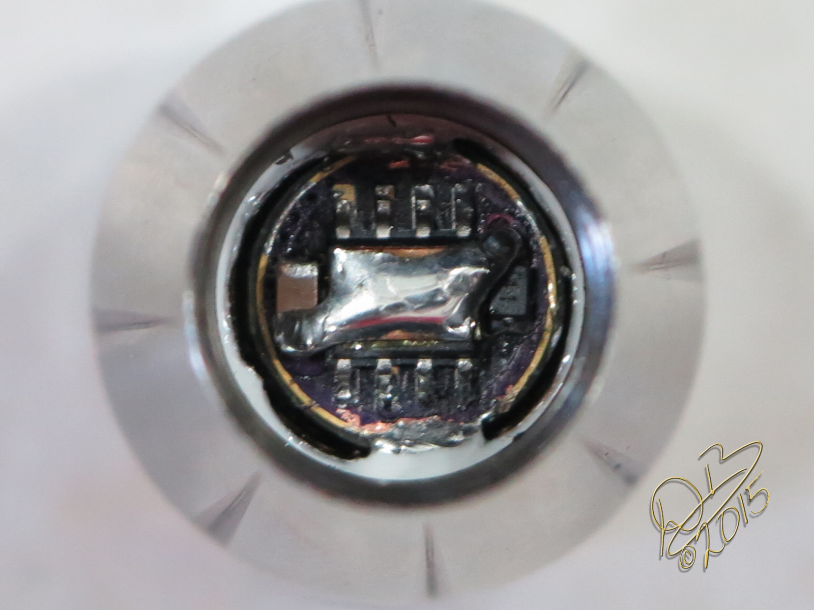
This is actually an MTN 17mm driver with the positive contact in the middle.
Hmm… so you did… I see that we had a PM conversation covering that topic called ":-) retaliatory try this! :-)" back in October 2014.
So… in that case who identified the SiR800DP? Eh, apparently me heh… at the time I found it I must have recalled that PM conversation and thought that SiR800DP was the one you showed me. (FWIW note that I later realized that the SiS414DN which I mention in that post uses a different package / eg is unsuitable.)
I’m certain that I have examined SiR404DP at some point, but I couldn’t tell you a thing about it right now. :-/
EDIT: And DB Custom (then DBCstm) must have done the leg work! I certainly wasn’t shelling out $2 for an FET at the time. ![]()
I bought my first 5 SIR800DP from Mouser on Dec 15, 2014 for $1.83 each. ![]()
With one left in my kit, I have used 114 of the SIR800DP since that first purchase. ![]()
Used a lot of PSMN0R9 and 3R0 as well, and a few Toshiba thrown in for good measure. ![]()
Where’s the smiley with the big, wide, and alarmed eyes when you need it? Good stuff DB Custom.
I vaguely remember the Toshiba ones… they had a unique package with more metal involved. And maybe they cost around $3/ea? I dunno.
I bet that you’ve assembled more drivers in one day than I have total. ![]()
The Toshiba had a second metal plate on the top, not to be used for current but to be connected to a thermal mass.
I just did 25 in 2 panels the other day. Love doing em on a panel, looks so cool! Richard, now, is really REALLY making some drivers!

Sometimes I just do one, I have a small piece of sheet copper that I clamp in short straight stats and hold that in my vice, apply the soldering iron underneath. Occasionally I’ll reflow an emitter that way as well, if just doing something simple and quick.
Edit: Might be worthy to note that when I was just starting to populate those 25 boards it was storming and our lights went out. I used the 10,000 lumen BTU Shocker with triple 9V MT-G2s doing a ceiling bounce to be able to see to populate em. Later, when we got electricity back, I re-flowed them simultaneously on the stove top. ![]() Yet another light with a AW driver in it. :bigsmile:
Yet another light with a AW driver in it. :bigsmile:
For the record, the tiny 10mm FET’s with MMU and crazy small MOSFET’s are a PITA! The MMU has to be re-flowed onto a programming chip board, then taken off and put on the driver. All 7 components, virtually the same as our normal drivers, fit on a 10mm board. Those can drive ya bonkers!