It's a slow ramp on the FET gate charge which repeats forever. It goes from 'invisible' to 'a bit too bright to look at directly' on a BLF-A6 FET+1 driver. From the spec sheet, your small FET should charge much more quickly as the gate charge is about 1/8th. You can avoid the higher end by reducing the '150' loop counter. Slow down the ramp by increasing the '200' delay. If the steps are too large, a CPU frequency of 9.6 MHz instead of 4.8 MHz should help. And if it's still too bright, PWM could be done with some work. Oh and keep an eye on the FET if you run this, it could get fairly hot at moderate output.
How this would behave with a depleting cell depends on the output voltage of the boost circuit at near zero load (ie. I don't have a clue). On a li-ion setup I can compensate for the lower voltage with more charge. Could perhaps do something similar here if there was a voltage readout, which I understand would be tricky to fit in there. The other "fix" is to just have more modes.
Also, I've never tried this but the weird code could be probably replaced with regular PWM and a resistor of the right value between the PWM pin and the FET gate. I'm not sure about the component sizing (not my domain and seems very tight) but ideally, I think you could keep pin 6 as it is and connect pin 5 to the FET gate via through a resistor, or the other way around. That would make one PWM channel pulse the FET full on for the high modes and the other give the FET only partial charge for the low modes. It would be much easier to adapt current dual-PWM firmware that way. A simple matter of disabling output of the unused PWM pin for any given mode.
A completely different option would be to keep the "full on" short FET pulse but with lower frequency to reduce the PWM duty cycle. You can get N times lower output by decreasing PWM frequency by a factor of N. But it will become ugly at some point. It is also somewhat annoying to code, like what I posted above.
Anyway, this long rambling post is just to say there are options so don't worry too much about current lack of a very low mode. I hope I didn't write anything too crazy :)
Ordered some of each board. Hopefully, I will have the time to join in on the testing. Has anyone identified a low cost source for the inductors in the US?
I just ordered my allotment of boards from OshPark and forgot to order the 17mm set of these. Will have to get a set on the next order, wanted to test in a P60! These look very interesting.
I just don’t have the time right now to read all the separate threads on this topic. Mostly, I just want to know what range of smd footprints will work with these boards.
Regarding inductance rating. I see recommended above 4.7uH. In another thread there is a pic that says it has a 2.2yH, Coilcraft XFL4020 used. Was yH a typo? Sorry for the newbie questions but I haven’t spent any quality time with inductors and don’t have time right now to do so. I only understand what they do at a high level.
@fixed it
That sounds promising.
I admit I understood only every second word of what you said, but i’ll dig into it.
I’m no firmware guy but I usually can adapt what others come up with.
.
@ImA4Wheelr
Here in EU these Coilcraft inductors even increased in price about 70% in the last 12 months. They were expensive back then, they need to be weighed in gold by now.
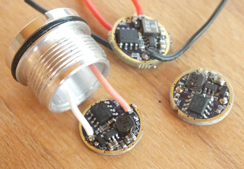
Any other inductor with the µH-specs and size should do, I tried several (look at my 3rd pic in post#4).
The other (non-Coilcraft 2.2µH) inductors have mostly higher DC-resistance and thus are less efficient, like, losing some 5-10% output in 1AA and (some) runtime in 2AA.
All inductors I tested (same board, swapped inductors, same cell, measured output current; very humble and unprecise testing scenario) did work on the Nanjg110. Only difference I experienced was efficiency.
Datasheet does not say above 4.7µH, it says minimum 2.2µH, 4.7µH recommended. All commercial driver of this kind I recollect have 2.2µH inductors. I tried 4.7µH and the only difference was that they were less efficient at similar size (as they have by design a higher resistance than the 2.2µH). 4.7µH might/will have advantage in other terms (saturation?) but i wouldn’t know anything about it. I’ll stick with 2.2µH. You can take the inductor from the FT-driver for starters.
y makes for µ on a keyboard without a µ.
.
@mattlward
Allow for 12-15 hours and you get another 17mm driver board to choose from.
Good point.
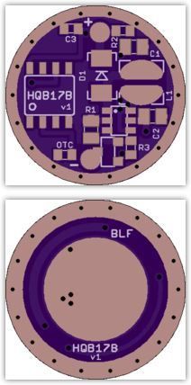
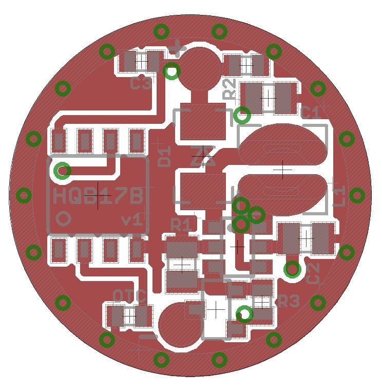
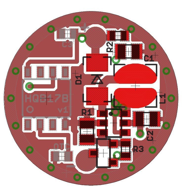
I added the SMD part sizes in the HQB15 v3 post. All HQB15 (v1/v2/v3) have the same parts.
In the HQB17 v1 post the footprints are stated. Notable difference is the larger inductor.
.
Yep, oncoming HQB17B is specifically meant as the simplest possible part swapping build (keeping fingers crossed that C2 will be sufficient).
Output should be in the 750mA range with 2AA. Very well within the spec of the PAM2803. Output depends on R1 (Sense Resistor) and the FT driver has R1 = 0.120 Ohm (“R120”), could change with any production batch, as always.
- The code I posted is to test the behavior of the FET with a partially charged gate. Quick & dirty way to see low output. Don’t leave it running too bright too long.
- Plan B: It can be integrated into other firmware for low modes, with some difficulty.
- Plan A: The hardware can be changed a little to get similar low modes with slightly modified existing attiny13a firmware. The resistor value can be approximately worked out from behavior of the code I posted.
Plan C: Use lower PWM frequency. Also complex but definitely possible and with no hardware changes. Has risk of visible PWM eventually. Might eat up valuable firmware space.
The major unknown is how much the results of A & B will depend on part variations. I’ve not done enough testing to have any clue. It could be that each driver must be flashed with different settings to get the same output. I think that would be annoying but still better than no low modes at all.
Yeah, some clarity about output expectations for 1xAA or 2xAA would be nice. Also, I don’t know anything at all about driver development. Does this need a custom firmware written for it, or do (any/all) the already available Tiny13 firmwares work? I’ve been trying to follow along, but I’m way over my head.
That is a very interesting approach, fixed it, thanks for posting! Most spend their time trying to bypass triode, not linger in it. Like you said, it'd be interesting to test what kind of dissipation occurs if you drive it that way and whether the trade-off in efficiency is worth it.
This isn’t about high power. Output remains the same and is limited by the power handling ability of the boost ic to ~1A Max or lower by choice of sense resistor. What’s new is the addition of the Attiny 13A. This opens all the AA and 2xAA cheapo and not so cheapo lights up to mods without annoying strobe modes or with modes of choice. Non muggle modes for muggle lights.
It’s time for some field testing.
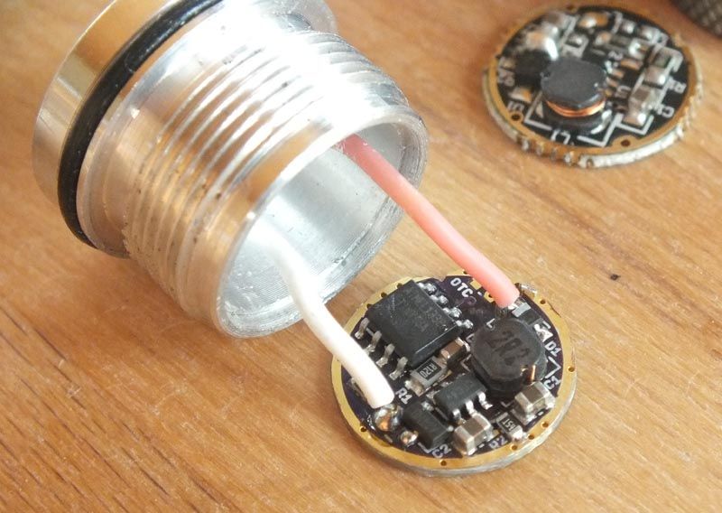
I just built a HQB15 v2 and installed it in a Sipik SK68 clone.
First memorable result: A swap of the FT driver will need additional capacitance (higher C2 or additional C3).
I did at first a straight transfer of only the FT parts and got only initial flickering. Like: strobe for half a second. Same after every mode change. I changed between different driver frequencies, still just flickering.
The FT driver had 10µF as C2 (10.7µF according to DMM, I tested it after harvesting the part). Added a 10µF 0603 (tested 7.8µF) as C3 and - voila - the light stays bright in every mode.
R1 is 0.120 Ohm (R120), no ‘overclocking’ for now.
Flashed is the already mentioned adapted MiniDrv with 3 modes (PWM 1,8,255), with on-time memory (no OTC).
I started with 4.7kHz (9.6MHz, fuse 6a (divider:8), fastPWM) and now flashed to 38kHz (9.6MHz, fuse 7a (divider:1), fastPWM). Both work, 4.7 is whining considerably and has higher low, 38kHz is silent and slightly better at PWM1.
Let’s see how it handles some heavy use. Pics later.
Edit:
Of course I swapped for a BAT60A before installing into the SK68, as the original diode was only attached by wire.
I successfully built one HQB15 v3 and one HQB17B v1, which both are running fine in lights. Still with simple firmware, I tweaked the MiniDrv firmware with several mode groups which took me a lot of time.
To be honest I at least postponed the idea for LVP. None of my AA light has it and I can live with a dead or degraded eneloop once in a while. I just won’t find the time to dig deeper here. I will finish the planned 17mm LVP boards (C/D) so if anyone else wants to progress LVP he has something to go on. Just ask if you need a certain layout.
I started working on HQB15M and this one looks really promising in Eagle so far. Made me chuckle more than once. I redesigned my Attiny MMU breakout board and that took me a while, but now it all might get into shape.
Using the Attiny13a-MMU would even allow for sub-15mm variants. Just sayin’