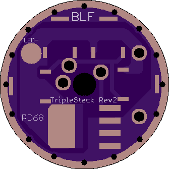
I should add, there are non-ground pads very close to the edge, so before inserting in a pill you will probably want to wrap some kapton around the circumference
Wow, I’ve missed out on a great thread thread. Guess I’ve been avoiding drivers and FW for quite some time now.
EDIT: 7135’s like to be kept cool. Especially, on fresh cells. You may want to think about moving them to the top of the bottom board where they will have a better heat sink path.
Good tip, but that would mean i addition to the two batt+ wires and grnd wire, I would have to run two pwm wires too….
I think I’ll try it like this for now and see what happens. What I really should do is source some of those square brass pins for a more stable stack.
How many solid header pins do you think it would take to carry the same current as 18awg stranded wire?
Edit: one standard 0.025”header pin is the equivalent of a 21awg. So for those of you that would actually use this, is it better to have a big hole to feed some silicone wire through, or 2-3 holes for these pins? This is for the ground connection between driver and contact board.
My thought is that the pins will give it better heat management. It would also provide a good structure for a potted driver.
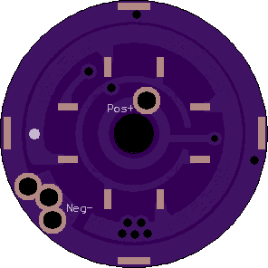
I should have been more specific. Only the large set of 7135’s should be moved down to the bottom board. One or two on the top board should be able to dissipate their heat via the surface area of the upper driver and through the copper wires connecting to the bottom board. The bottom board doesn’t need a Batt. You can just run Batt straight from the spring to the top board/LED. Both the top and bottom board need Batt~~. So that wire would remain. All you need in addition to that is PWM feed and LED~~. So 3 wires total.
Oh.
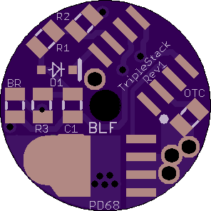
Normally I try to make my drivers as useful as they can be for people other than myself, but I thought I would be the only one who liked the idea of the pins. So I did it “my way”. This involved reducing the driver size by 0.5mm (15mm now), removing 2 of the 7135’s (I usually only use 3 anyways), and removing the FET pulldown resistor (I’ve yet to need one, and they’re easy to stack on the FET pins themselves) . You can use just about any 0.025” header pins you want, but I ordered these just now.
Why did you have to remove the 7135s? You could split the placement of the three pins. 1 or2 where they are now. 1 at the via for r2. And one at the via for the bleeder resistor. You would need to move the bleeder via and the fet output just a bit to make that happen. The ground ring on the bottom of the driver board should be enough to carry the signal. What do you think?
Guessing those pins will be gold coated steel. If so, they will be rigid, but will conduct heat and electricity less efficiently. That much rigidity doesn’t seem needed. Some flex will help protect the solder joint from breaking. 22 gauge solid copper wire will be a tad over .025”. Here is a chart showing the diameter of various gauge wires:
I was under the impression the pins were brass. They come in either tin plated or gold plated. Even so, I’m assuming they will have more resistance than copper wire (which is partly why I thought the whole idea was going to be unpopular).
I had to remove one of the 7135s, and I chose to remove another one just because I personally never use more than 4 and I didn’t think anyone else would be using this board. I wasn’t even planning on posting it here to be honest.
I don’t think I can move the vias for the pins. To put them where the other smaller vias are would mean I have to make the driver bigger again, which will push the pins more outside, and I think that would cause clearance issues where the contact board sits on the shelf of the pill.
You should know that if you build it they will come ![]() all your work seems to dictate the BLF fads. Just saying people like what you do
all your work seems to dictate the BLF fads. Just saying people like what you do ![]()
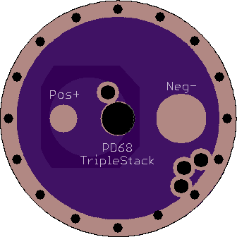
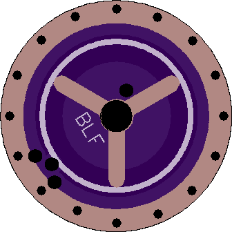
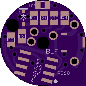
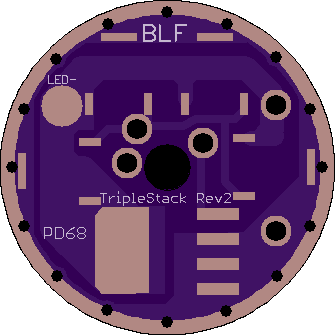
I think this was the hardest puzzle I’ve ever done. Things are very tight to say the least. Still an even 15mm for the top board, but we are back up to 5 total 7135’s. Most of them are on the bottom board for better heatsinking, as is the FET. The FET pulldown resistor (R4) is back and C2 from the Q8 has been added (it is optional) to go with the input resistor (R3). The bleeder resistor is gone but I can count at least 3 places you can stack one if you need to. This version uses 5 header pins, but none of them will carry more than 380mA. Your emitter wires will be mounted to the spring and contact board and will bypass the stacked board entirely. This one should be easier to get a programming clip on, and it consists of two single-sided boards for easier reflow. Both boards are required for function but I left them as separate files so that you can order the bottom board thick and the top board thin.

Wow! Very nice! I think this board will be perfect for the d80. I have 25 d80s to modify. The driver has to be one sided on these lights because of the retaining only thing that would be nice is an 18.5mm contact plate. That’s just for my purpose though.
I wasn’t happy with how messy those traces were, so I cleaned some things up. I think I’m about to order; the OP will be updated too. Feel free to follow this maze to check the circuit if you’d like to. It’s not my prettiest, but should be functional.
Order Links:
15mm Top board
17mm Contact board
18.5mm Contact Board
20mm Contact Board


Thanks PD! I will order some. Will lpak56 fet fit on the contact board or what fet is needed?
Yep, standard S08 FET pads like most of my boards
The funny thing is, what we consider ugly and sub-par is actually quite good by most compact PCB standards.
Good work!
Really? That’s surprising. Just having the MCU tilted to one side at an odd angle drives me nuts. I’m the type of person that likes things to be uniform and symmetrical if possible.
I also just realized this one would be even easier to drive a secondary LED (like red) than the original was. Just don’t connect a header to the top right via and use that for a second LED- wire instead.
Yep, it also annoyed me at first then I started looking at some other compact PCB designs and realized that most appear to just use the auto-placement / auto-router and thats it.
As I am sure you know, the auto-placement and auto-router are just beautiful things to behold (for everyone else I am being sarcastic, they are downright ugly to look at).
Fact is those setups work just fine even with 5 times more vias then they need and traces 3x longer then can be done.
So I decided after that to just get it on the board and make it as pretty as was possible in a reasonable time frame. Once it is in the light I only care about how it works anyways.