You should know that if you build it they will come ![]() all your work seems to dictate the BLF fads. Just saying people like what you do
all your work seems to dictate the BLF fads. Just saying people like what you do ![]()
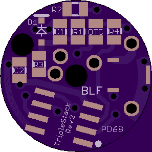
I think this was the hardest puzzle I’ve ever done. Things are very tight to say the least. Still an even 15mm for the top board, but we are back up to 5 total 7135’s. Most of them are on the bottom board for better heatsinking, as is the FET. The FET pulldown resistor (R4) is back and C2 from the Q8 has been added (it is optional) to go with the input resistor (R3). The bleeder resistor is gone but I can count at least 3 places you can stack one if you need to. This version uses 5 header pins, but none of them will carry more than 380mA. Your emitter wires will be mounted to the spring and contact board and will bypass the stacked board entirely. This one should be easier to get a programming clip on, and it consists of two single-sided boards for easier reflow. Both boards are required for function but I left them as separate files so that you can order the bottom board thick and the top board thin.

Wow! Very nice! I think this board will be perfect for the d80. I have 25 d80s to modify. The driver has to be one sided on these lights because of the retaining only thing that would be nice is an 18.5mm contact plate. That’s just for my purpose though.
I wasn’t happy with how messy those traces were, so I cleaned some things up. I think I’m about to order; the OP will be updated too. Feel free to follow this maze to check the circuit if you’d like to. It’s not my prettiest, but should be functional.
Order Links:
15mm Top board
17mm Contact board
18.5mm Contact Board
20mm Contact Board


Thanks PD! I will order some. Will lpak56 fet fit on the contact board or what fet is needed?
Yep, standard S08 FET pads like most of my boards
The funny thing is, what we consider ugly and sub-par is actually quite good by most compact PCB standards.
Good work!
Really? That’s surprising. Just having the MCU tilted to one side at an odd angle drives me nuts. I’m the type of person that likes things to be uniform and symmetrical if possible.
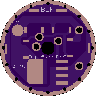
I also just realized this one would be even easier to drive a secondary LED (like red) than the original was. Just don’t connect a header to the top right via and use that for a second LED- wire instead.
Yep, it also annoyed me at first then I started looking at some other compact PCB designs and realized that most appear to just use the auto-placement / auto-router and thats it.
As I am sure you know, the auto-placement and auto-router are just beautiful things to behold (for everyone else I am being sarcastic, they are downright ugly to look at).
Fact is those setups work just fine even with 5 times more vias then they need and traces 3x longer then can be done.
So I decided after that to just get it on the board and make it as pretty as was possible in a reasonable time frame. Once it is in the light I only care about how it works anyways.
“auto-placement and auto-router”? … never heard of her. ![]()
I lay every trace using either the line, circle, arc, or square tools.
Though I must admit, this was a lot easier when we had 7 parts on our drivers, they all easily fit on one side of 17mm, and it didn’t matter where they were in relation to each other. DEL’s scope has made my life so much harder ![]()
I just have to laugh though. Between the few revisions I did that was the most difficult board I’ve ever done, and it was all just so I can use a bigger spring….
LOL, I guess eagle doesn’t have any automation features for placement or trace routing? They are no good for small boards like this in diptrace but I messed around with them at first, downright ugly layouts but it worked.
So eagle just sees the layout as a picture not much different then MSpaint? I guess that is why I could not get the hang of it.
Diptrace sees each pad, trace, copper pour and via as there own part and it knows exactly what should connect to everything else. so while I still have to layout the placement and traces manually it takes care of all the small things because it knows what goes where.
I will agree that the extra parts make things a lot more interesting, thats why I went with 0603 resisters, they are not much harder to work with, even hand soldering and are just as good as the 0805 versions for a performance standpoint for our uses.
Eagle does have fancy stuff, I just don’t use them. The way I do it, yes it’s basically just a multi-layered bitmap.
You can link a schematic to a board and have it check your circuit for you, and give suggestions and treat traces as signals and such, but I didn’t know what I was doing and it would just give me errors all day long. So early on I figured out that if I just skip the schematic, it will let me draw traces wherever I want without complaining about all of the “rules” I was breaking. Since that’s how I’ve been doing it since day 2, I have never learned the more advanced features of Eagle. That’s also why my files usually aren’t much help to people that want to learn the “right” way.
I don’t mind working with 0603, but my small stockpile of parts are all 0805 and I didn’t want to buy all new stuff.
Yeah, once you learn a way of doing something it is hard to relearn. Thats why I generally take a rather long time to pick out which program I will use for a new format, (like solidworks for CAD, diptrace fo PCB, photoshop for jpeg, DXO for RAW ect.)
There is nothing wrong with doing it like you do, just harder to keep track of things during the design process and if you make changes to the parts later it is harder to update them. So it is a tradeoff.
Thanks PD! Ordered some triple stack boards. If it works well I will be ordering a bunch of them.
cool cool. You ordered the top board in 0.8mm, right?
I just ordered some too. Hopefully the thin boards don’t take too long extra
Texas_Ace, Eagle has an autorouter that tries its best to optimize the signal path. I have seen it do some weird looking stuff. But, it seems to be able to get traces to places I couldn’t figure out how to reach. I’ve never seen an autoplacement button, but I’m a very new user, so I could have missed it. Sometimes, as PD said, the fancier features actually make things harder when you already know how and where you want to place things.
PD, if you start to get bored with easy stuff, and want something more challenging, try looking at my contest light driver. It’s my first attempt, so maybe I’m still in the learning curve and that makes everything seem hard. But, I’d like to make that monstrosity with no traces on the bottom, just one huge ground plane. I’ve utterly failed so far. I did get a board designed, but it’s super ugly and has traces popping up and down through vias all over. I don’t even know how to do the correct placement of parts. I read about DEL’s scope and know there were changes made to the Q8 driver because of it. But, I just don’t know what I’m doing. Your drivers always look so nicely laid out. It is funny that you did all this work, and had such a difficult time, all because you just wanted a bigger spring.
Glutton for punishment I guess.
I’ll take a look at your thread
Pretty cool looking boards. Ordered a set of 17/15mm in 2oz. Thank you PD.
Yup. Ordered in .8mm