Nanjg AK-47C20 help please

I have soldered drivers before, just not this type. Four questions.

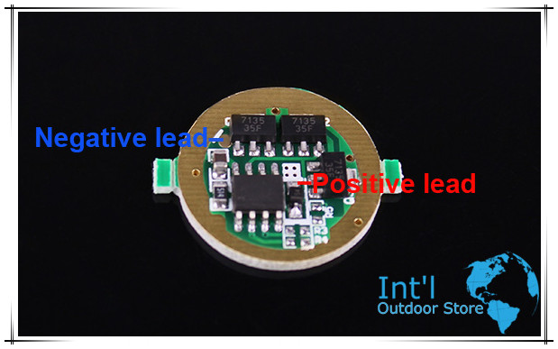
1. Is the “plus” (positive) solder point the little blob of solder in the picture …… OR is it really the little white square with holes in it? I’m thinking the little white square as the holes seem to go through the PCB and end up on the large positive (plus) solder point on the reverse side of the PCB (where the spring will go). But I’m probably wrong. They design these chips so that the smallest possible area is the assigned solder point, which would make it that eentsy tiny blob of solder, of course.

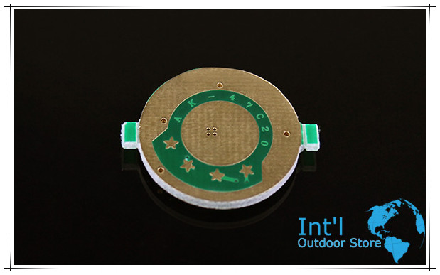
intl-outdoor says solder the stars produces different mode selections. They say:

1st Star : Low (10) - High (100)

2nd Star: Low (5) - Medium (30) - High (100%)

3rd Star : Low (5) - High (100) - Strobe

4th Star : Low (5) - Medium (30) - High (100%) - Strobe – SOS

2. And which is the “first” star: The first one on the left or the first one on the right?

3. I connect the star with a solder “blob” to the outside (neg) circular solder point to activate whatever mode group I want? Or is it the inside (plus) solder point?

Reminds of ye olde PC days when motherboard manufacturers gave you just enough info to have to guess and possibly ruin a $200 m-board. Approximately 25 more words and the instructions would have been bulletproof clear.

4. FINALLY: With this driver, will a U2, U3 or T6 emitter make any noticeable difference in brightness, or will the T6 be about the same as the U2 or U3?

As always, thanks to everyone for their help. Yes, I could have asked intl-outdoor, but I figured BLFers might have some other jewels of wisdom about this driver.

Its the square pad with holes.

From left to right.

You connect the star to the outer - ring

U3 > U2 > T6, each will be roughly 7% brighter than the next lower bin, but you wont see any difference by eye, unless you have them side by side.

But I wonder what modes you get without any star connected. My guess is that you would have the same modes as with star 1 connected..

1. It's the tiny solder blob. But you don't have to be that careful about it.

2. ???*

3. To the outer ring.

4. Depends.

* I originally wrote "right to left", but NightCrawl is probably right.

I originally said:

>>>>>>>>1. Is the “plus” (positive) solder point the little blob of solder in the picture ……
>>>>>>>>OR is it really the little white square with holes in it? I’m thinking the little white square as the
>>>>>>>>holes seem to go through the PCB and end up on the large positive (plus) solder point on the
>>>>>>>>reverse side of the PCB (where the spring will go). But I’m probably wrong.
>>>>>>>>They design these chips so that the smallest possible area is the assigned solder point,
>>>>>>>>which would make it that eentsy tiny blob of solder, of course.

One respondent says: 1. Its the square pad with holes.

Another says: 1. It’s the tiny solder blob. But you don’t have to be that careful about it.

Can someone break the tie? :wink: My soldering pen is heated up with nowhere to go.

I've never tried the square pad by itself, but I guess it would work too. Sometimes I use just the small blob and sometimes I use both the blob and pad and get the same results. I think the small blob and the square pad are actually the same point in the electrical path.

LED current is controlled via - path on these drivers. So you want to connect the LED to battery +. And thats where these holes (=vias) are. The tiny solder blob belongs to the reverse polarity protection diode for the MCU.

Make sure you use flux on your star of choice they can be a PIA to get to bridge to the outer ring.

>>>>>LED current is controlled via - path on these drivers.

WOW!!! Interesting. I +KNEW+ I would get the definitive answer here on BLF. Thanks!!!

>>>>So you want to connect the LED to battery +.

And since that solder pad with the holes is knocking against the plus battery terminal, you can’t get any closer to the plus battery poles than that! Thanks again. and thanks to everyone who answered the questions.

QUESTION: And now for another question that will REALLY show my OCD. Are those tiny holes to better hold the solder? Or should I actually try and and work a couple wire strands through them for a better solder bond?

This driver appears to have some of the biggest soldering pads that I have seen so far. Shouldn’t be too bad at all. I’ve seen some that are like dust specks and are not made for 61-year-old eyes.

>>>>>>Make sure you use flux on your star of choice they can be a PIA to get to bridge to the outer ring.

Yup, didn’t even think about that. Trying to trace that string of solder across that green pcb could be tough. Before this I have always just relied on what’s in the solder. Erik, do you have a recommended flux brand or type? Do you just put it on the star OR draw a little line with it from the star to the outer ring?

I’ll practice on a few fried drivers.

There's this explanation by Dr. Jones of the ak-47 from a while back:

But your driver is a ak-47C20, I suppose it is the 20mm version of the ak-47C driver, the stars in that one have no function, mode-group changing is done with the switch, see the review of the ak-47C by sixty545

That white is part of the silk screen/solder mask… it’s paint. Can’t solder to paint. You have to make the connection to the small metal pad. Also, if you tried to solder to the white square with the holes, solder would work it’s through the holes and stick up a bit on the other side, reducing the area where the battery can contact the driver.

I have some old Radio Shack Rosin Soldering Paste Flux I use Cat. No. 64-021A

I put a blob on the star than one on the ring than I put another blob on top to connect the two.

Bridging the gap with a little piece of wire works also.

@djozz: Sadly its not that simple with products from China. :D I would rely on the description given by IO, they were always correct so far.

@texaspyro: Thats of course also possible. But I have used similar drivers with "white" pads before and the solder stuck to it. You never know for sure.. Lets see what the OP finds out.

Those holes in the pad are there to bring the connection to the other side of the board, no need to fill them or run anything through them.

in the few 7135 drivers I’ve used, I really struggled to solder the LED wires on to those tiny pads, so for the +ve pad I just scraped the white paint off that square, tinned it and used that. Was a lot less stressful :slight_smile:

I wish more drivers came with through hole contacts, they’re much easier to get a good connection to for the solderingly challenged.

I successfully did 2 mods with these drivers (2 Jacobs):

1 - The L+ is as noted on the pic from Dr Jones, which matches I-O's pic (not the white pad w/holes)

2 - The "1st star" is the right most with the stars on the bottom -- this will match what's documented in Dr. Jones post above.

3 - solder the star to the outside ring -- I used a short piece of wire, soldered at each end - it's too long of a distance for solder alone, at least at my skill level

4 - well, this is a low amp output driver for XML's at 1.05A. I would add 7135's piggyback'ed to get it up there. Double up each and you got 2.1 - add 2 stacked on a stack and you got 2.8A (2 of 3 triple stacked). I would think at the same tint (1A for example), you should do better with a U3, but typically U3's are only available at 1C. I don't know -- 1.05A for an XML is really, really low - I got T6, U2 and U3 lights but nothing at that low amperage.

Also, in 2 mode I did extensive testing and found it does seem to have mode memory, contrary to the description on the I-O page. If I turn it off on high, it comes up in high next time, whether it's 1 minute or 1 day later. I got my Jacob in 2 mode at 2.45A (1 triple stacked) -- it's nice now but I'm waiting on a XR-E R5 EZ1000 from Kaidomain but FastTech has them cheaper, supposedly.